Grant Conditions Binding Host Designs Using Unshielded Limited Transmitters
Unshielded limited transmitter grants bind host manufacturers to strict PCB layout, power rail, and chamber re-test protocols before compliance is recognized.


Leak
Near-field radiation from bare circuit components couples directly into nearby conductive structures on the host board. In standard full modular approvals, an integrated grounded metal enclosure surrounds the radio frequency circuitry to contain stray energy and block outside interference. If a manufacturer seeks authorization without this shield, regulatory authorities reject standard modular certification and issue a limited approval instead, shifting electromagnetic containment duties onto the host board developer.
Federal Communications Commission guidance under KDB 996369 D03 and Innovation, Science and Economic Development Canada provisions under RSP-100 Section 8.4 enforce specific operational constraints when a radio lacks independent shielding. Without an enclosure, high-frequency harmonic currents transfer directly into neighboring microstrip lines, supply traces, and high-density logic components. Host circuit traces acting as unintended parasitic antennas then radiate spurious emissions beyond the legal limits set by FCC Part 15 Subpart C or ETSI EN 300 328.
| Approval Classification | Physical Shielding Requirement | Integration Binding Mechanisms | Host Retest Obligation |
|---|---|---|---|
| Full Modular Approval | Integrated metal shield required over all radio frequency components. | Standard integration instructions supplied by radio vendor. | Basic host verification scan for unintentional radiation. |
| Standard Limited Modular Approval | Physical shield present; non-compliance involves supply voltage regulation or buffering. | Contractual agreement binding host supply voltage or interface logic. | Spot-check radiated scans targeting fundamental and harmonic bands. |
| Unshielded Limited Modular Approval | No physical shield present on the transmitter module assembly. | Strict grant conditions binding host printed circuit board layout and enclosure geometry. | Full radiated spurious emissions re-evaluation in the final host housing. |
Radio frequency energy escaping unshielded power amplifier stages induces surface currents across adjacent ground fills. These return currents flow along path lengths dictated by host PCB geometry rather than module design. When host return paths exhibit high impedance at harmonic frequencies, the entire mainboard acts as a radiating dipole, meaning compliance in a standalone test fixture provides no assurance of compliance inside a final product enclosure.
Integration instructions for unshielded transmitters lay out exact spatial keep-out zones, copper pouring requirements, ground via density, and trace routing restrictions. Standard modular rules assume metal shielding; altering specified layout parameters changes the radiated electromagnetic profile and invalidates original laboratory measurement data. The host manufacturer becomes legally responsible for transmitter compliance the moment the unshielded assembly mounts to a custom mainboard.
Proper trace separation on the host mainboard eliminates the need for an integrated metal shield.

Regulatory Conditions Binding Unshielded Integration
Regulatory grants issued for bare RF assemblies establish legal boundaries that transfer radio compliance liability directly to the host equipment manufacturer. Under the Federal Communications Commission framework, an unshielded radio receives a limited modular grant containing explicit conditions precedent. These conditions restrict installation to specific host configurations evaluated by the original grantee or require the grantee to maintain direct operational control over all host designs.
Standard modular grants permit flexible integration across arbitrary host designs, whereas limited unshielded grants restrict host geometry to maintain compliance boundaries.
Documentary requirements under KDB 996369 D04 require host integrators to archive engineering evidence proving strict adherence to the grant conditions. System integrators maintain these engineering records throughout the commercial life of the product. Market surveillance audits by telecommunication certification bodies demand proof that host PCB trace dimensions, component spacing, and layer stack-ups strictly mirror the baseline design certified during initial approval.
Non-compliance with KDB 996369 D03 host integration instructions renders the final product an uncertified intentional radiator, triggering immediate border confiscation.
Host product manufacturers must incorporate specific compliance statements and regulatory identifiers directly into documentation and product labels. European radio approvals under the Radio Equipment Directive 2014/53/EU require host manufacturers to execute a full risk assessment under Article 3.2 when integrating unshielded radio assemblies. Simply collecting a Declaration of Conformity from the module vendor fails to establish host compliance when physical radio shielding is absent.
- Grant Condition Mapping Document containing line-by-line verification of host PCB physical layout against original module testing parameters.
- Host Spot-Check Test Report capturing radiated spurious emissions data from an accredited testing facility across operating channels.
- User Manual Mandatory Declarations specifying exact FCC identifiers, ISED certification numbers, and user exposure distance statements.
- Engineering Change Control Log tracking all mainboard layout revisions, layer thickness variations, and power supply decoupling modifications.
Under Section 15.212(b) of the FCC rules, host integration of a limited module requires a formal agreement specifying the exact host PCB configuration validated during certification.

Coupling
Parasitic energy transfer between unshielded radio components and nearby digital signal paths generates severe harmonic distortion across radiated test bands. High-frequency magnetic fields generated by the module power amplifier inductor induce unwanted noise currents into adjacent host trace loops. Without a metal shield to terminate flux lines, magnetic coupling falls off slowly over physical distance, forcing host designers to establish wide isolation zones around the radio footprint.
Closer trace placement increases spurious energy. Multilayer host boards require continuous, uninterrupted reference ground planes directly beneath the radio assembly. Slots, splits, or cutouts in underlying copper layers force return currents to travel around obstacles, creating high-frequency loop antennas that elevate radiated emissions beyond regulatory limits.
Solid ground planes beneath unshielded modules absorb near-field capacitive currents and return them efficiently to the primary power source.
A three-millimeter reduction in host ground plane clearance increases secondary harmonic emissions by 8.4 dB at 4.8 GHz.
Power supply decoupling presents a primary path for conducted noise propagation in unshielded configurations. The absence of local module filtering allows RF currents to enter host power rails, modulating digital clocks and sensor lines. Host designs incorporate dedicated low-pass filtering networks comprising ferrite beads and low equivalent-series-resistance capacitors directly at the radio power input terminals to prevent power ripple from degrading transmitter performance.
- Route the unshielded transmitter power supply lines through dedicated inductor-capacitor filtering arrays situated within five millimeters of input pins.
- Maintain continuous copper ground fills on all internal layers beneath the radio footprint without routing signal traces across ground split regions.
- Place stitching vias at maximum three-millimeter intervals along ground plane perimeters to seal microstrips against stray electromagnetic pickup.
- Position high-speed digital buses and switching voltage regulators on mainboard layers isolated by solid ground shields from the radio assembly.
Solid unbroken ground planes beneath the radio section suppress host board parasitic noise far better than localized shield cans added after layout completion.

Validation
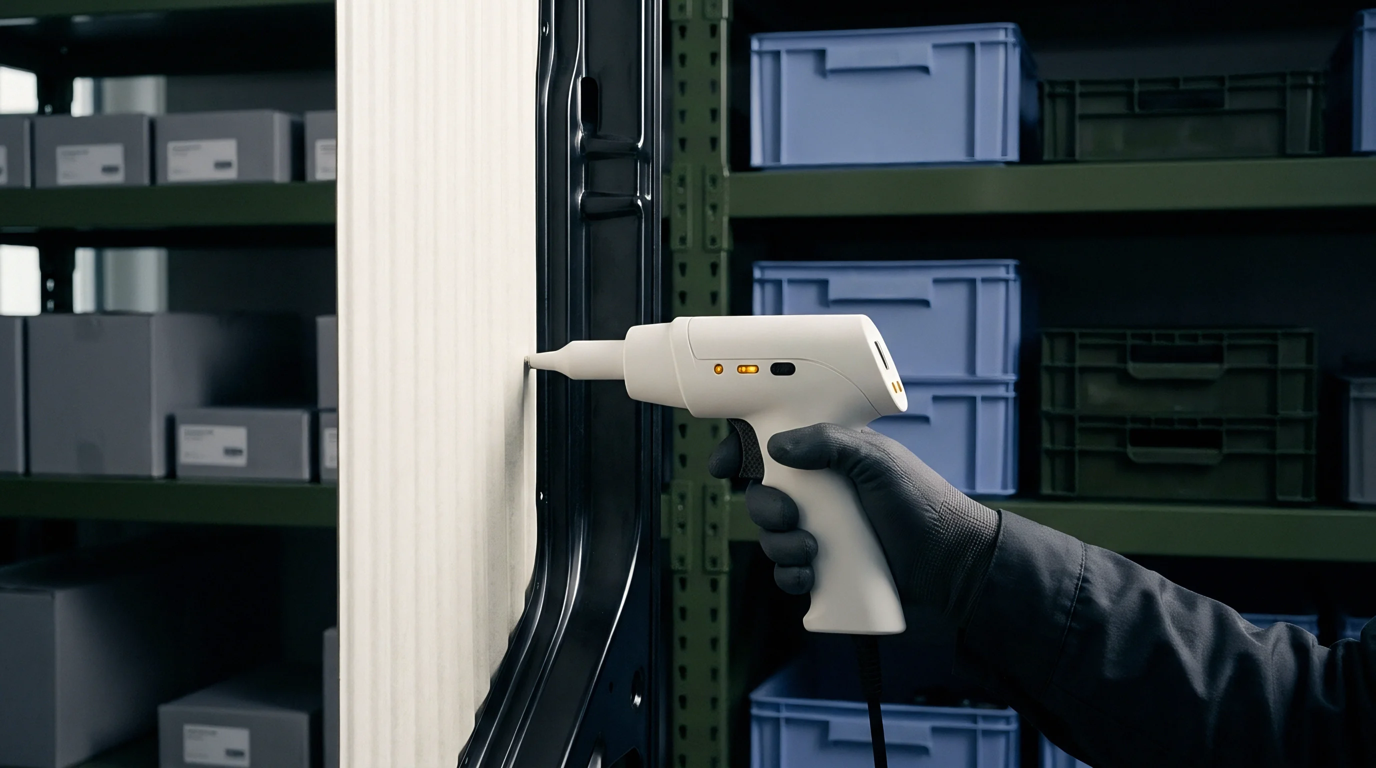
Laboratory measurement of host integration requires systematic radiated spurious emission scans while operating the unshielded transmitter at maximum rated power. Test engineers place the assembled host equipment on a non-conductive turntable inside an anechoic chamber. Antennas sweep vertical and horizontal polarizations while the turntable rotates through three hundred sixty degrees to capture peak emissions across fundamental and harmonic frequencies.

What Host Modifications Trigger a Class II Permissive Change?
Modifying host mainboard layout, changing enclosure material, or altering power supply circuitry often invalidates original test data for unshielded limited modules. The Federal Communications Commission classifies layout deviations that elevate radiated emissions as Class II Permissive Changes under KDB 996369 D02. A permissive change requires formal filing with a Telecommunication Certification Body along with fresh chamber test data showing the host product maintains compliance under modified conditions.
| Design Modification Area | Threshold Deviation | FCC Administrative Action | Re-Test Requirement |
|---|---|---|---|
| Host Ground Plane Geometry | Reduction in area exceeding 5 percent or movement of ground vias. | Class II Permissive Change (C2PC) | Radiated spurious emissions sweep from 30 MHz to 10th harmonic. |
| Enclosure Material Composition | Transition from metallic or shielded material to unshielded plastic. | Class II Permissive Change (C2PC) | Radiated emissions check and maximum permissible exposure assessment. |
| Antenna Trace Routing | Trace length variation exceeding 1 millimeter or impedance shift over 5 percent. | New Equipment Authorization or C2PC | Conductive power, occupied bandwidth, and band-edge compliance scans. |
| Power Supply Source | Substitution of linear regulator with high-frequency switching regulator. | Class I or Class II Permissive Change | AC power-line conducted emissions scan under FCC Part 15.207. |
In cases where host layout changes severely alter transmitter radiation patterns or elevate harmonic levels past regulatory thresholds, a Class II permissive change proves insufficient. Regulatory agencies then mandate a completely new equipment authorization filing under a unique regulatory identifier. Obtaining a new grant incurs substantial administrative fees and introduces long testing lead times that delay market entry, push back shipping schedules, and risk customs hold-ups.
Pre-scan radiation sweeps performed early in host layout reveal stray harmonics before expensive final certification testing begins.
Failing to execute spot-check testing on the host board leads to suspension of market authorization and forced product recalls from retail channels.

Expense
Commercial realization of products incorporating unshielded transmitters demands realistic financial accounting of host verification fees and certification timeline buffers. Integrating bare RF circuitry lowers upfront module purchasing expenses relative to fully shielded units. That initial unit-cost saving transfers development budget directly into regulatory compliance, custom board iterations, and extended chamber testing hours.
Consider a commercial IoT device incorporating an unshielded Wi-Fi and Bluetooth combo radio module. The host mainboard requires custom multi-layer PCB design to satisfy grant conditions. Standard fully shielded modules allow fast-track four-layer host board design and require basic verification testing costing roughly four thousand dollars across two days in an accredited chamber.
The unshielded module demands a six-layer host mainboard with precise controlled impedance and controlled ground plane dimensions, increasing raw PCB tooling and unit fabrication costs.
Chamber fees accrue rapidly during retests. Initial pre-compliance scans for the unshielded host assembly reveal unwanted third-harmonic radiation coupling onto an adjacent display ribbon cable. Remediating this leak requires board trace layout modifications, additional grounding shielding strips, and a second round of chamber pre-scans.
The financial buildup follows a structured trajectory across regional markets:
- Anechoic Chamber Hourly Rates running from three hundred to five hundred dollars per hour, accumulating over twenty to forty hours during re-scan sweeps.
- Class II Permissive Change Filing Fees charged by Telecommunication Certification Bodies, ranging from eighteen hundred to three thousand five hundred dollars per jurisdiction.
- In-Country Representative Fees mandated for overseas markets such as South Korea or Brazil, costing twelve hundred to twenty-five hundred dollars annually per filing.
- Local Accredited Laboratory Retests required by Giteki or KC certification regimes, adding six thousand to twelve thousand dollars in mandatory local testing.
Filing administrative processing adds four weeks per target market. When an unshielded host fails initial radiated spurious limits, re-engineering PCB layout and executing secondary testing shifts product commercial launches by eight to twelve weeks. Missing an established retail ship window results in liquidated damages, distributor penalties, and lost market share that outstrips original module cost savings.
Host testing for unshielded limited transmitters doubles overall chamber hours compared to standard fully shielded modular integrations.
Unshielded radio integration proves cost-effective only when production volumes exceed one hundred thousand units, where unit-level bill-of-materials savings absorb elevated compliance expenses. At lower production volumes, the accumulated cost of custom PCB stack-ups, permissive change filings, and extended chamber time renders unshielded radio integration commercially unviable.
How international standards bodies will harmonize host re-evaluation criteria for unshielded millimeter-wave modules remains an unresolved challenge for cross-border hardware sourcing.