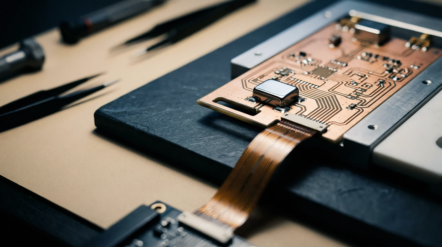
Meaning
Printed circuit board landing areas designed to connect with leadless packages utilize flat metal surfaces positioned beneath the component body. Using bottom-terminated pads allows manufacturers to achieve high functional density in compact hardware assemblies. These interfaces eliminate traditional gull-wing leads, bringing the semiconductor package closer to the underlying substrate.
Thermal Coupling
Heat dissipation relies on the direct contact between the silicon housing and the copper plane on the circuit board. Because bottom-terminated pads minimize the thermal resistance path, they operate efficiently under heavy electrical loads. This direct path prevents the device from overheating during continuous operation.
Manufacturing Risk
Solder voiding occurs frequently due to the escape of volatile flux gases during the reflow process. For bottom-terminated pads, this trap leads to joint degradation.
Quality Inspection
X-ray imaging provides the primary method for evaluating the completeness of the subsurface connection after assembly. Since visual inspection cannot reach underneath the component, automated transmission x-ray systems must verify the absence of bridging and voiding before final product approval. This non-destructive test confirms that the hidden joints meet IPC acceptability criteria by revealing the distribution of the solder alloy across the pads.
Furthermore, it establishes a reliable baseline for long-term vibration resistance.