Meaning
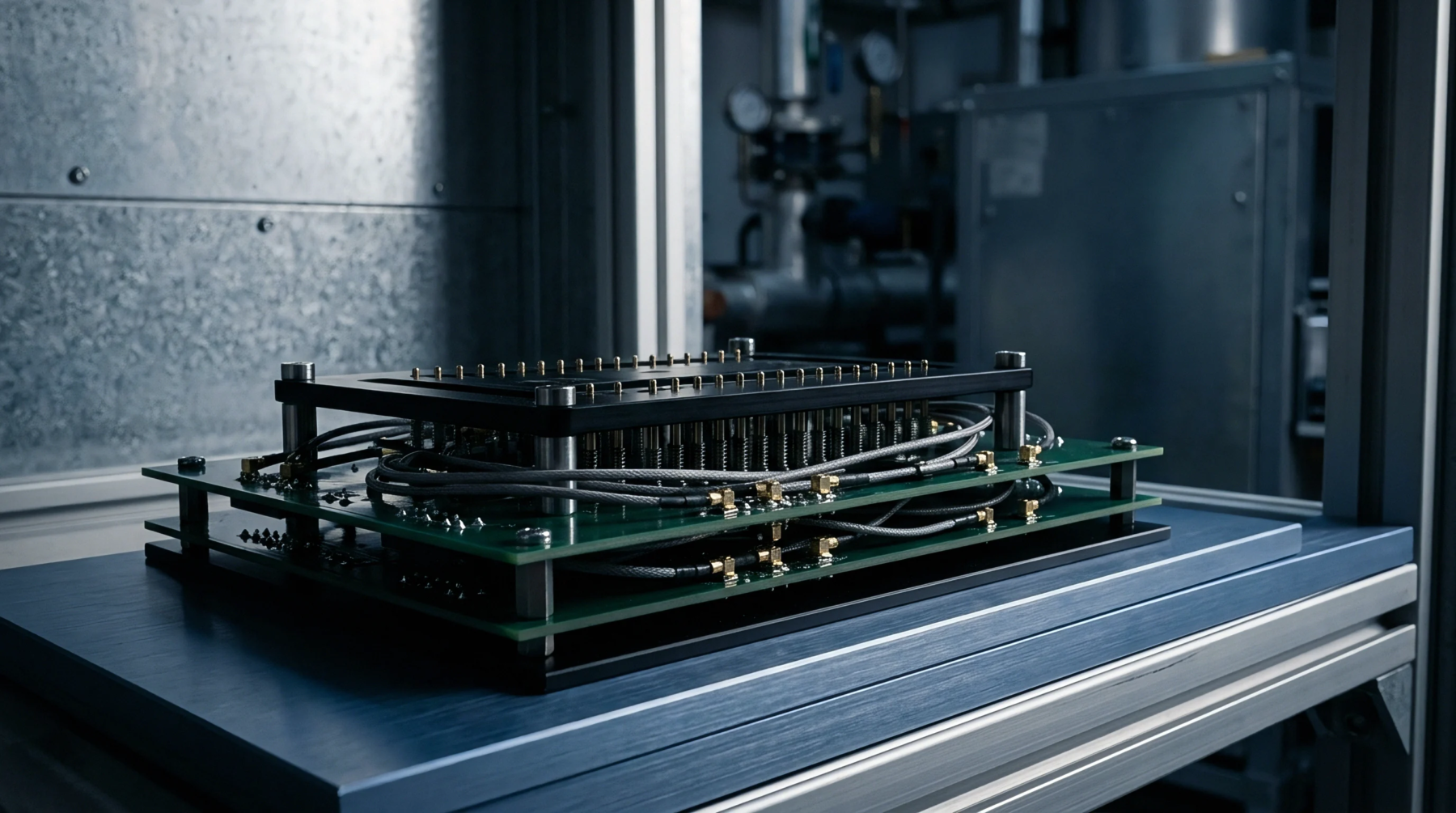
Measuring the electrical performance of two complementary transmission lines is essential for validating high-speed communication interfaces. Engineers use differential pair testing to evaluate how well a balanced signal line pair suppresses common-mode noise and maintains signal integrity. This evaluation is necessary for high-speed protocols such as USB and PCIe, where skew and attenuation must be minimized.
The test results confirm whether the board-level design meets the electrical standards of the targeted standard.
Physical Measurement
High-performance oscilloscopes and network analyzers are required to probe the microstrip or stripline routing on the PCB. During differential pair testing, researchers inject complementary signals and measure the resulting waveform at the receiver end. Proper probe placement and calibration are necessary to prevent instrument-induced distortion from skewing the results.
This step validates the physical layout of the transmission lines.
Parameter Extraction
Scattering parameters characterize how the signal behaves across a wide frequency range. Analyzing these values reveals return loss, insertion loss, and differential-to-common-mode conversion, which should be minimized.
Defect Detection
Discontinuities in trace spacing or dielectric thickness along the routing path generate reflections that degrade the signal eye diagram. Through differential pair testing, engineers can isolate physical faults such as asymmetric trace lengths, solder bridge issues, or micro-cracks in the copper plating. These flaws cause intra-pair skew, which transforms part of the differential signal into common-mode electromagnetic interference.
Resolving these defects before mass assembly ensures compliance with emissions regulations and guarantees high data throughput in the finished enclosure.