Meaning
Semiconductor packaging design attaches an inverted active die directly to an organic or ceramic substrate using micro-bumps on the face of the silicon. Utilizing a flip chip ball grid array eliminates the need for peripheral wire bonds, which reduces parasitic inductance and maximizes connection density. This packaging design is bounded by the pitch of the bottom-side solder balls, which are soldered to the system printed circuit board during reflow.
Interface Interconnect
The direct connection between the die and the substrate minimizes signal transit times and improves high-frequency performance. Distributing the micro-bumps across the entire surface of the die allows for a vastly higher number of input and output pins compared to traditional edge-bonded packages. This structural layout is essential for high-performance processors and radio-frequency chips that require low-resistance power distribution and clean signals.
Thermal Dissipation
Heat is removed efficiently from the back of the exposed silicon die because it sits on top of the assembly without intervening molding compound. Engineers attach heat sinks or metallic shields directly to this exposed silicon to maintain safe operating temperatures. The package rating is determined by the thermal resistance of this direct contact pathway.
This pathway must be carefully designed to prevent thermal hotspots from degrading the performance of adjacent wireless circuits.
Board Assembly
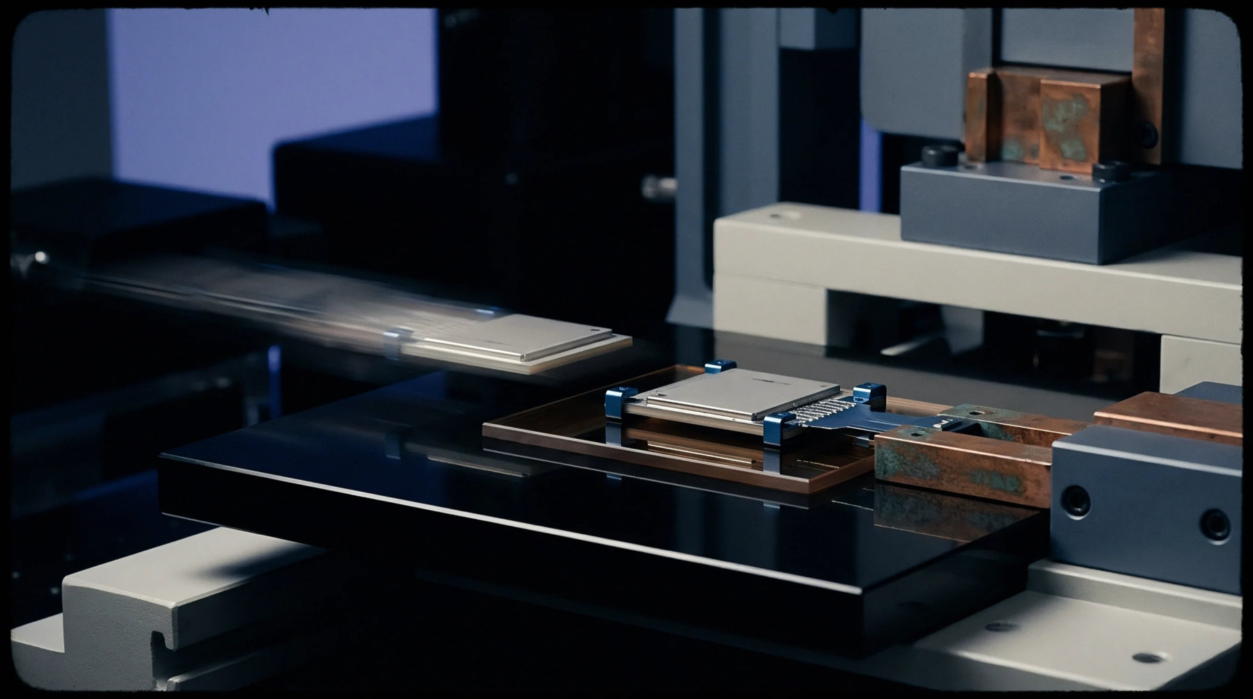
Automated pick-and-place machines position the package onto the circuit board with high precision before it travels through the reflow oven. The surface tension of the molten solder balls helps self-align the package to the copper pads of the board during this heating process. After assembly, the mechanical stability of the interface is evaluated through thermal cycling tests.
These tests expose the assembly to temperature extremes to ensure that differences in the thermal expansion coefficients of the silicon, substrate and circuit board do not cause joint failure.