Meaning
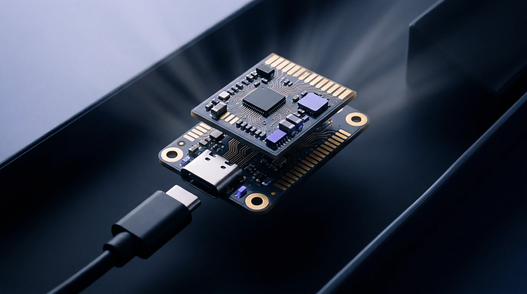
Inverting integrated circuit dies directly onto substrate carriers eliminates wire interconnections to minimize parasitic inductance and package footprint. The flip-chip interconnection methodology places solder bumps or copper pillars over the entire active surface of the silicon die. Array connections across the die surface enable higher input and output density compared to peripheral bonding methods.
Parasitic Mitigation
Traditional peripheral bonding relies on fine gold or aluminum wires that introduce several nanohenries of loop inductance. Replacing these wire loops with short solder joints reduces connection inductance to under one hundred picohenries in a flip-chip package structure. Lower inductance prevents ground bounce during rapid switching of high-speed digital outputs.
Power distribution networks benefit from low-resistance planar interconnect arrays that maintain steady voltage supply rails under dynamic loads.
Thermal Management
Heat dissipation improves when silicon dies couple thermally to substrate materials through dense arrays of solder joints. Backside cooling plates attach directly to the exposed die surface of a flip-chip assembly without wire loop interference.
Assembly Qualification
Solder joint reliability under cyclic thermal stress determines product longevity in consumer and industrial devices. Engineering teams subject assembled boards to temperature cycling tests to verify joint integrity across environmental extremes. Underfill materials injected beneath the silicon die distribute mechanical stress caused by thermal expansion mismatches between silicon and substrate.