Calculating Base Module Unit Economics for Standard Wireless Interfaces
Base wireless module unit economics balance silicon bill-of-materials costs and testing yields against the volume needed to dilute fixed certification capital.

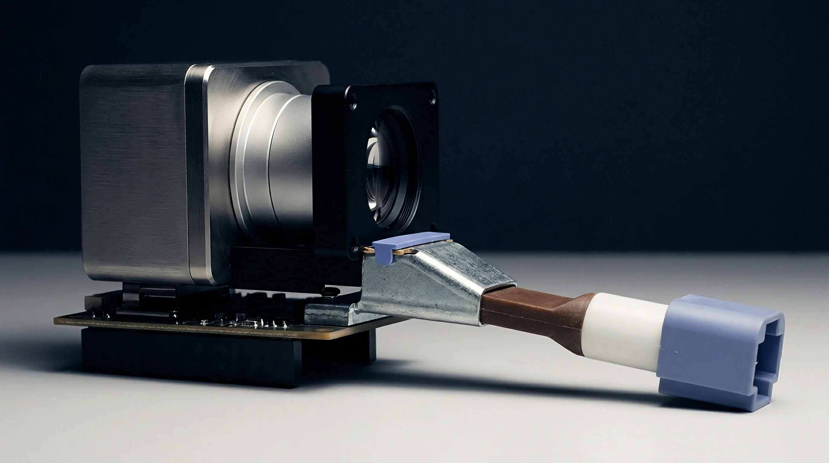
Silicon
Radio-frequency integrated circuit pricing sets the floor for any module bill of materials. Below one hundred thousand units, an IEEE 802.15.4 or Bluetooth Low Energy system-on-chip with on-chip power management and thirty-two-bit processing runs between 0.72 dollars and 1.15 dollars from Taiwanese or European silicon foundries. Dual-band Wi-Fi 6 silicon with dual-stream multiple-input multiple-output transceivers occupies a much higher bracket, opening between 2.45 dollars and 3.80 dollars.
Base silicon marks the direct material ceiling; packagers build upward from there with matched passives, higher-order harmonic filtering, crystal resonators, and printed high-density interconnect substrates.
Substrate choices settle base yields before pick-and-place equipment ever handles a die. Four-layer FR-4 host materials cost roughly 0.03 dollars per module unit in high-panelization layouts. High-frequency RF laminates like Rogers RO4350B or modified polyimide drive board costs to 0.18 dollars per unit, but they curb dielectric losses across five-gigahertz transmission paths.
Discrete passives then widen the bill of materials: a standard Bluetooth module pulls in roughly thirty-five discrete components ~ 0201 decoupling capacitors, tuning inductors, and balun structures ~ adding 0.09 dollars. Sourcing a thirty-two-megahertz main crystal resonator with ten-parts-per-million tolerance alongside a thirty-two-point-seven-six-eight-kilohertz sleep crystal adds another 0.14 dollars per unit.
A thirty-two-megahertz crystal with ten-parts-per-million tolerance adds fourteen cents to base material expenditure under room-temperature conditions.
Packaging technology creates wide cost spreads between wire-bonded plastic quad flat no-lead packages and flip-chip ball grid arrays. Wire bonding carries modest tooling charges on standard capillary machines running gold or copper wire. Flip-chip designs call for wafer bumping, flux application, and tight reflow profiles, raising assembly processing costs by roughly twelve percent while cutting substrate footprint by half.
The trade-off is spatial density versus tooling commitment.
A buyer laying down bare silicon directly on the main board takes on full responsibility for thermal dissipation and RF ground return paths. A module supplier handles assembly fallout internally, building that attrition directly into factory margins.


Shield
Deep-drawn tin-plated cold-rolled steel cans isolate low-noise amplifiers from board-level digital noise and keep harmonics out of unlicensed industrial bands. The stamped metal barrier itself carries a trivial raw material price of 0.04 dollars at volume. The real commercial impact settles into two downstream areas: surface-mount placement cycle time and radio compliance testing overhead.
Soldering a two-piece shield with an independent clip frame enables secondary factory rework, whereas seamless one-piece soldered lids force complete scrap whenever internal ball alignment fails inspection.

Why Do Certified Modules Command Premiums?
Regulatory certification shifts expensive laboratory exposure off the device integrator. Full modular certification across Federal Communications Commission Part 15 subpart C and Radio Equipment Directive requirements demands fifty thousand to eighty thousand dollars in non-recurring test expenses when pursued chip-down on a host product. Pre-certified canned modules eliminate host-level intentional radiator filings, reducing final system testing to unintentional radiator verification under fifteen thousand dollars.
Laboratory amortisation shapes unit pricing across manufacturing runs. Distributing seventy thousand dollars of certification expenses over twenty thousand devices adds three dollars and fifty cents per device. Sinking that same fee across five hundred thousand units dilutes the regulatory impact to fourteen cents per device.
| Interface Standard | Silicon BoM | Passive Components | Shield And Passives | Modular Test Overhead | Pre-Certified Unit Price |
|---|---|---|---|---|---|
| BLE 5.3 (1 Mbps) | $0.78 | $0.12 | $0.06 | $0.15 | $1.85 |
| IEEE 802.15.4 (Thread/Zigbee) | $0.88 | $0.14 | $0.07 | $0.18 | $2.10 |
| Wi-Fi 4 (1×1 2.4 GHz) | $1.10 | $0.22 | $0.09 | $0.24 | $2.45 |
| Wi-Fi 6 (1×1 Dual-Band) | $2.15 | $0.48 | $0.14 | $0.38 | $4.65 |
| Wi-Fi 6E / 7 (2×2 Dual-Band) | $4.20 | $0.85 | $0.22 | $0.65 | $8.90 |
Automated optical inspection flags cold joints under shield fences before secondary RF calibration starts. Shield wall thickness has to reconcile stiffness during tape-and-reel feed with finished component weight. Can deflection under high-speed vacuum nozzles shorts against internal decoupling passives, and rework costs escalate quickly once the lid bonds permanently to the perimeter trace.
When high-frequency shielding is miscalculated, parasitic capacitance detunes the matched antenna trace and forces an expensive physical respin of the circuit substrate.


Volume
Tooling commitments separate low-run evaluation builds from multi-year manufacturing runs. Tooling non-recurring engineering fees cover stencil laser fabrication, component placement program optimization, and dedicated multi-site RF test fixtures. Standard automated test equipment for wireless modules incorporates four-channel spectrum analyzers and vector signal transceivers, commanding hourly operational run-rates upwards of ninety dollars.
Test duration per unit determines factory throughput ceilings.

Are Discrete Reference Designs Viable for Small Runs?
Skipping production-grade RF verification invites catastrophic field failure rates. Checking a dual-band radio across transmit power, error vector magnitude, frequency tolerance, and receiver sensitivity ties up bench gear for thirty to forty-five seconds per unit. Module vendors amortize that test fixture investment over hundreds of thousands of standard catalogue devices.
Replicating those test jigs for an in-house chip-down build takes thirty-five thousand dollars in bed-of-nails hardware and test automation development.
ETSI EN 300 328 wideband transmission standards establish clear radiated power ceilings that penalize imperfect transceiver board layouts.
Break-even economics clarify when an engineering team abandons pre-certified assemblies to build discrete transceivers directly on host circuit boards. Calculating this transition demands factoring upfront capital against marginal delta savings.
- Tooling Amortisation establishes baseline capital requirements for automated surface-mount assembly, including steel stencils, feeder setup, and automated optical calibration profiles.
- Regulatory Verification generates substantial external laboratory invoices for intentional radiator authorizations under global radio equipment regulations.
- RF Optimization consumes specialized engineering man-hours tuning antenna matching networks, filtering unwanted harmonics, and verifying return loss through vector network analysis.
- Test Jig Deployment demands capital investments in programmable RF power meters, shielded isolation boxes, and automated test firmware routines.
The unit economics illustrate the pivot point. Take an industrial telemetry board using Wi-Fi 4 single-stream connectivity. A pre-certified module invoices at two dollars and forty-five cents at ten thousand units, whereas the discrete silicon layout bills at one dollar and thirty cents in raw components ~ a delta of one dollar and fifteen cents.
Recovering that difference means absorbing eighty thousand dollars across intentional radiator filings, five-layer RF host revisions, and dedicated factory test fixturing. That eighty-thousand-dollar expense measured against a one-dollar-and-fifteen-cent margin delta yields a break-even point near sixty-nine thousand five hundred units; below that volume, buying the module preserves capital.
Tooling and testing hardware remain tied to the specific factory floor where bring-up occurs, which limits sudden production transfers to competing board assembly houses.


Margin
Contract manufacturing tiers establish predictable margin markups above raw bill-of-materials expenditures. Tier-three contract manufacturers handling low-to-medium runs apply component markups between eight and twelve percent, paired with surface-mount placement charges of 0.008 dollars to 0.015 dollars per joint. Tier-one manufacturers handling millions of assemblies drop component markups down to three percent, using high-speed dual-lane surface-mount placement lines that reduce placement cost to 0.003 dollars per solder joint.
Scrap allowances introduce additional friction; surface-mount line reel-loading procedures mandate two percent excess component allowances on 0402 and 0201 packages.

Whose Balance Sheet Absorbs Yield Drop?
Yield loss on RF lines hurts far more than dropped digital logic. A loose microcontroller pin flagged after reflow can be reworked with localized hot air. An assembled module exhibiting phase noise drift or spurious out-of-band harmonics under a soldered can is scrap.
Scrap rates on wireless module manufacturing lines hover near three to five percent during initial ramp phases, settling down to one point two percent under steady-state production.
A complex two-by-two MIMO radio assembly rarely achieves higher than ninety-six percent first-pass yield during initial pilot runs.
Factories balance these operational risks by layering specific contract mechanisms into their commercial volume agreements.
- Target Yield Caps define the specific percentage threshold below which the assembly plant absorbs component scrap penalties directly.
- Component Price Variance provisions allocate fiscal responsibility for unexpected silicon broker markups or raw quartz market fluctuations during long-term runs.
- Test Socket Attrition schedules dictate billing cycles for high-frequency coaxial pogo-pin replacement across thousands of repeated mating cycles inside RF testing enclosures.
| Tier Level | BoM Markup | Cost Per SMT Joint | Target Line Yield | Scrap Allowance |
|---|---|---|---|---|
| Tier 3 (Sub-50k Units) | 10.5% | $0.011 | 97.2% | 2.5% |
| Tier 2 (50k-250k Units) | 6.8% | $0.007 | 98.4% | 1.5% |
| Tier 1 (250k+ Units) | 3.2% | $0.004 | 99.1% | 0.8% |
Automated test equipment calibration drift regularly accounts for third-quarter factory margin surcharges.

Transfer
Buying an off-the-shelf catalog module buys time; running a clean design transfer secures supply independence. When moving from a turnkey vendor module to build-to-print or white-label sourcing, the transfer documentation is the asset. That release package has to be complete: Gerber RS-274X or ODB++ fabrication files, native schematics, pick-and-place centroid data, bills of materials with secondary sources for generic passives, and compiled factory test binaries.
Software and firmware ownership boundaries dictate post-transfer vulnerability. Silicon vendors supply software development kits under permissive BSD or proprietary Apache-variant software licenses, yet module integrators often embed closed-source bootloaders, factory calibration tables, and proprietary AT-command interpreters directly into on-module non-volatile flash memory. Lacking source access to calibration lookup routines, a buyer cannot bring up a secondary assembly facility.
The second factory cannot write correct frequency offset trims to raw crystals without the original vendor’s test software suite.
Standard development agreements reserve all factory test diagnostic intellectual property for the original module fabricator unless explicitly reassigned in writing.
Life-cycle exposure is where this bites hardest. A team holding custom firmware exercises full change control. If an upstream supplier issues an unannounced End-of-Life notice on an integrated low-dropout regulator, a customer without board-level design rights is stuck funding minimum lifetime buys.
Holding production Gerber files and native CAD databases allows swapping out obsolete discrete components within a routine engineering change order cycle.
IPC-1752A declaration standards govern material composition declarations for international compliance regimes, requiring suppliers to document exact chemical limits across every internal solder ball and dielectric core layer. Failure to secure full disclosure packages leaves import clearance vulnerable to sudden environmental tariff reclassifications at customs borders.
Whether secondary contract fabricators can maintain published phase noise specifications across replacement passive component vendors without redesigning matching networks remains an open engineering question.