Meaning
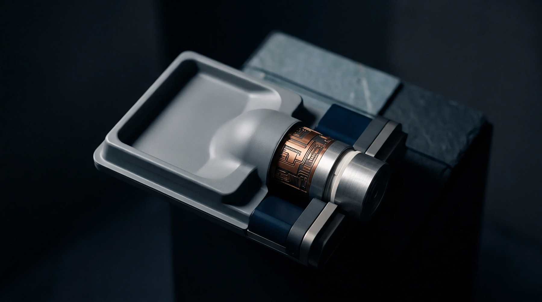
The engineered geometry of printed transmission lines forms the basis of microstrip design, which dictates high frequency signal routing on planar printed circuit boards. Conductor width, substrate thickness, and relative permittivity govern characteristic impedance and propagation velocity within the defined transmission structure. Copper traces bonded to dielectric layers above a continuous ground plane create the primary propagation path, while housing walls and nearby shielding structures establish the boundary where analytical field assumptions cease to hold.
Production validation relies on vector network analyzer measurements during final electrical test sequences to verify return loss against design simulation files.
Routing Constraints
Trace geometry optimization demands strict adherence to manufacturing tolerances set by board fabrication facilities. Etching variations alter trace widths, causing impedance shifts that degrade high frequency signal integrity across long board runs. Dielectric constant variations within the raw laminate material introduce phase velocity errors, forcing engineers to apply compensation techniques during layout generation.
Thermal expansion coefficients mismatch between copper foil and substrate layers during reflow soldering processes, creating mechanical stress along trace edges. Copper weight selection balances direct current resistance limits against high frequency skin depth phenomena, determining insertion loss performance.
Manufacturing Handover
Fabrication drawing generation requires explicit specification of copper thickness, trace width compensation, and dielectric stackup parameters. Board houses verify minimum spacing rules prior to film generation, ensuring etching processes yield predictable conductor cross sections. Electrical test fixtures utilize specialized probe footprints matching trace impedance to prevent measurement reflections during automated test procedures.
Visual inspection standards govern conductor edge roughness limits, because microscopic copper spurs act as high frequency resonance sites. Final assembly release occurs only after manufacturing data packages pass automated design rule checks without generating warning flags.
Thermal Budget
High frequency current concentration inside narrow copper conductors generates localized heating that alters dielectric permittivity values over time. Substrate materials degrade when operational temperatures exceed glass transition thresholds, permanently shifting circuit resonance characteristics. Copper weight selection directly influences current carrying capacity, preventing thermal runaway conditions within confined housing volumes.
Enclosure designers calculate conductive heat transfer paths from the printed circuit board to the outer chassis surface. Thermal cycling qualification tests expose the finished assembly to rapid temperature swings, verifying mechanical reliability of soldered joints along the transmission lines.