Meaning
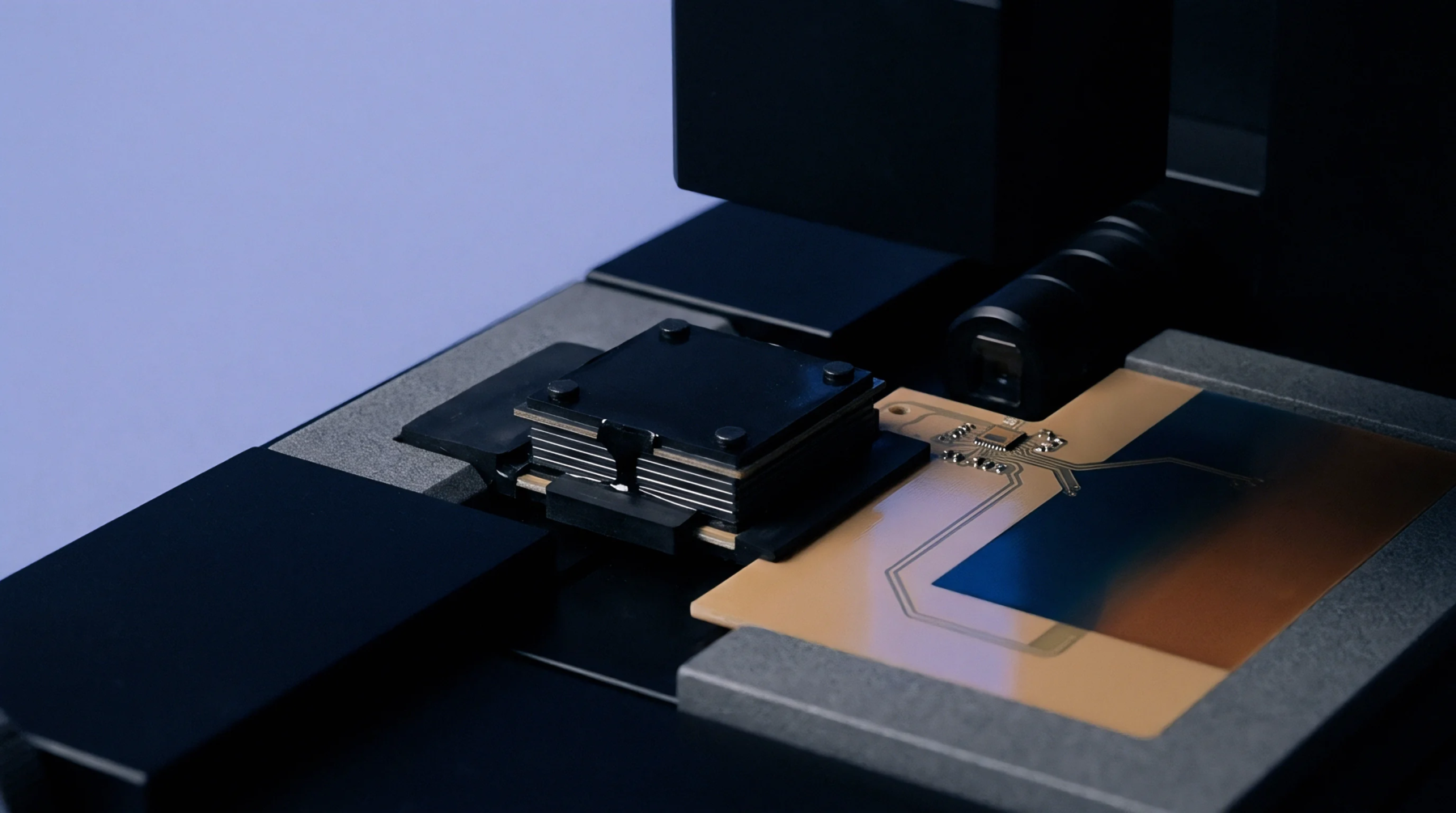
Automated testing of integrated optical and electrical devices on a wafer level requires precise alignment of fiber optics and electrical contacts. Through silicon photonics probing, engineers characterize the optical insertion loss, modulation bandwidth, and photodetector response before wafer dicing. The accuracy of this process is limited by the sub-micron mechanical tolerances of the alignment stages.
Alignment Precision
Positioning optical fibers next to on-chip grating couplers requires sub-micron resolution to avoid excessive coupling loss. During silicon photonics probing, automated alignment algorithms search for the peak optical power before initiating the measurement sequence. This step must be performed quickly to maintain high throughput in a production environment.
Interface Calibration
Calibrating both the electrical and optical test paths is necessary to isolate the performance of the device under test from the testing hardware. When executing silicon photonics probing, reference measurements on calibration substrates compensate for fiber-to-chip coupling losses and cable attenuation. This calibration ensures that the recorded data represents the true performance of the integrated transmitter or receiver.
Standardized test protocols are followed to guarantee repeatability across different test stations, which simplifies data analysis during wafer sorting.
Production Testing
Wafer-level characterization allows defective dies to be identified and marked before the expensive packaging stage. Performing silicon photonics probing at the wafer stage reduces the overall cost of manufacturing by preventing the packaging of non-functional optical chips. This screening is a standard practice for high-yield silicon photonics production.