Meaning
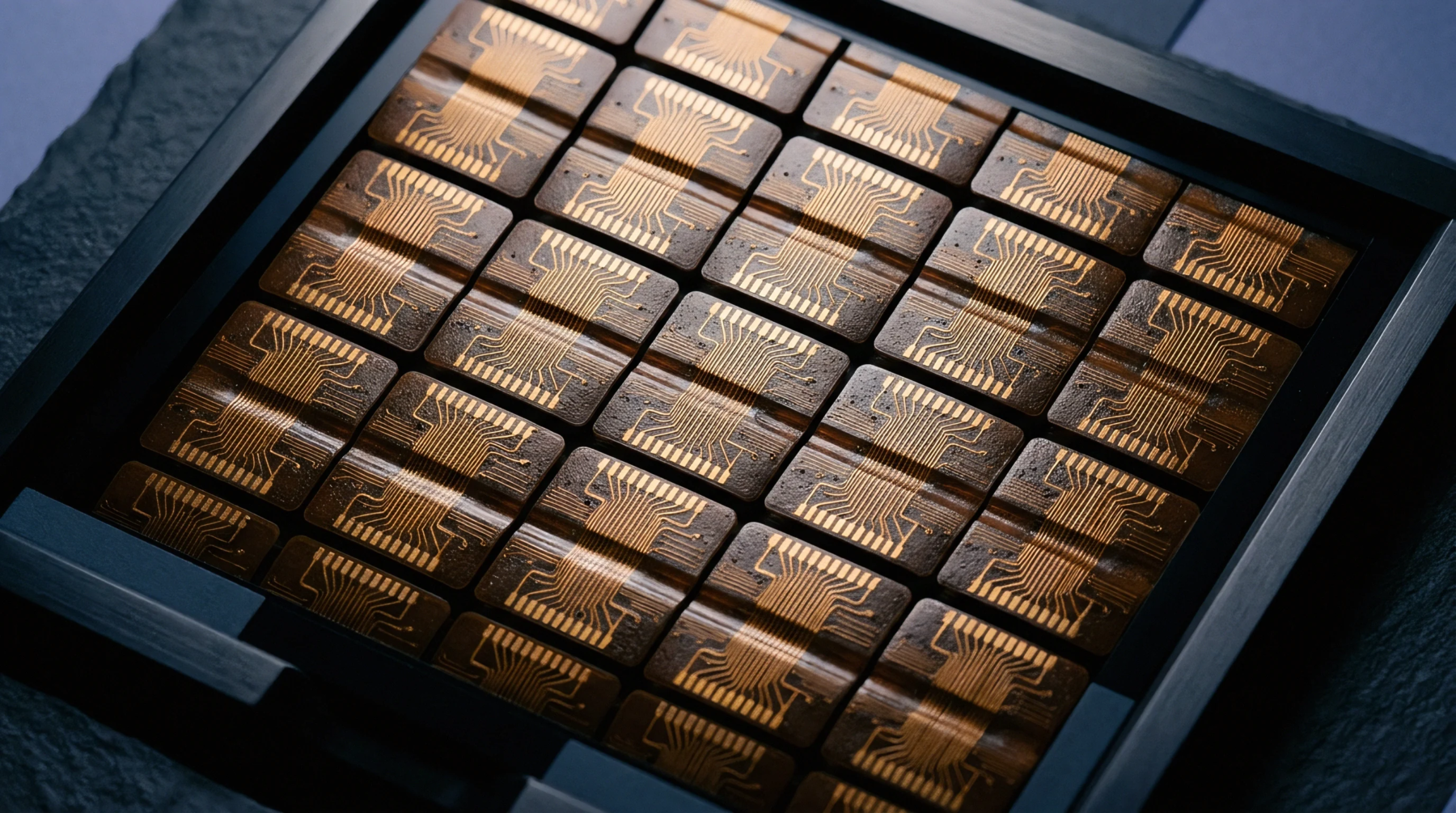
Base material layers made of high purity crystalline wafers provide the foundation for the fabrication of integrated circuits. Every modern connectivity module starts as a series of thin layers deposited on a silicon substrate to create the transistors and connections needed for radio communication. This material provides both the electrical platform and the mechanical strength required for the chip to survive the assembly process.
It is selected for its ability to handle high temperatures and its predictable electrical properties under different loads.
Electrical Performance
Structural integrity is maintained even as the wafer is thinned down to fit inside slim enclosures. The silicon substrate must be flat and free of defects to ensure that the microscopic patterns of the circuit are correctly transferred during the lithography phase. Any crack or impurity in the base material will cause the entire chip to fail its electrical test.
Structural Integrity
Performance characteristics such as electron mobility are determined by the way the crystal was grown and the presence of any dopants. Using a high quality silicon substrate allows for faster switching speeds and lower power consumption in the final device. This efficiency is a requirement for battery operated smart sensors that must last for years in the field.
Cost Basis
Thermal conductivity of the material helps move heat away from the active parts of the circuit during operation. The silicon substrate remains the most cost effective solution for the mass production of semiconductor devices.