Meaning
Physical disruption of an insulating medium occurs when an applied electric field exceeds the critical dielectric strength of the material, converting an insulator into a conductor. Across radio frequency circuits, printed circuit substrates and transmission line gaps, voltage breakdown produces destructive arcing or internal dielectric puncture that shunts signal energy directly to ground. Extreme localized current flow during the event causes thermal damage to board laminates and active device junctions.
The phenomenon defines the upper voltage limit of an electronic assembly, terminating normal component operation once dielectric recovery thresholds are breached.
Ionization Mechanism
Free electrons in the presence of strong electric field gradients accelerate to velocities capable of dislodging secondary electrons upon impact with neutral gas molecules or solid lattice atoms. This impact ionization initiates an avalanche process, creating an multiplying cascade of charge carriers across the insulation gap. In gaseous spaces, this progression culminates in Townsend discharge and continuous arc formation, whereas solid dielectric materials suffer permanent lattice bond rupture and carbonized conductive paths.
Voltage drops rapidly once the plasma or carbon filament forms.
Geometry Influence
Electrode contouring governs local electric field intensity far more than average potential differences across an assembly. Sharp trace corners and microstrip vias create concentrated field peaks that initiate corona discharges at voltages substantially lower than those calculated for flat plates. Designers use rounded conductor edges and guard rings to distribute electric field lines uniformly.
Spacing rules enforce minimum creepage and clearance distances across printed circuit boards.
Dielectric Verification
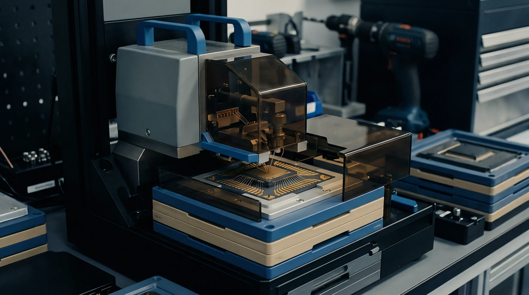
Manufacturing quality standards dictate high-potential dielectric withstand testing, commonly designated as hipot verification, to confirm insulation integrity between high-voltage rails and chassis ground. Test instruments apply direct current or alternating voltages at pre-determined safety margins above maximum operational ratings, measuring leakage current through insulating layers over fixed dwell times. Assembly technicians record breakdown voltage levels or leakage thresholds on product traveler sheets, rejecting any enclosure where insulation resistance drops below specified megohm values.
Environmental screening chambers repeat these electrical stress tests under high humidity and low atmospheric pressure conditions to detect spacing flaws before avionics or RF power modules receive final production acceptance. Completed test certificates confirm that dielectric barriers withstand transient overvoltage spikes without sustaining physical punctures.