Automating IPC-2581 Dielectric Stack-Up Verification during Secondary Factory Bring-Up
Automating IPC-2581 stack-up parsing aligns secondary factory laminate inventory with signal integrity targets, eliminating manual engineering delays and scrap.

Resin
An IPC-2581C file defines dielectric layers through structured XML tags that map physical lamination attributes directly into manufacturing data. High-speed designs depend on explicit glass weave styles, resin volume fractions, and pressed dielectric thickness parameters to meet tight signal integrity margins. Fabrication facilities, however, frequently carry different laminate inventories and substitute prepreg types to fit local supply chains.
Substituting 2116 prepreg for an original 1080 specification alters the bulk relative permittivity and dielectric loss tangent of the substrate, even if the total pressed height matches the CAD target.
Dielectric performance depends heavily on the ratio of glass cloth to epoxy matrix within the cured laminate. Glass filaments have a dielectric constant near 6.1, while pure epoxy resin falls between 3.0 and 3.4. When a factory replaces a resin-rich prepreg style with a lower-resin equivalent to reduce core spacing, the localized dielectric constant felt by high-frequency signals increases.
Because resin volume dictates final height and glass density alters attenuation, embedding the inner-layer copper foil profile complicates geometry further as copper fills open resin spaces during heat and pressure lamination.
| Glass Style | Nominal Resin Content (%) | Nominal Cured Thickness (mm) | Effective Permittivity (Er) | Dissipation Factor (Tan d) |
|---|---|---|---|---|
| 1035 | 75 | 0.071 | 3.45 | 0.0060 |
| 1078 | 64 | 0.079 | 3.62 | 0.0068 |
| 2116 | 54 | 0.117 | 3.85 | 0.0078 |
| 3313 | 58 | 0.102 | 3.76 | 0.0072 |
Variations in cured thickness shift conductor capacitance relative to reference ground planes. Etch factor distortions and copper tooth penetration depths displace resin during lamination, changing the actual distance between traces and ground. Automated verification scripts parse IPC-2581 stack-up definitions to calculate these physical variables before issuing computer-aided manufacturing tooling orders.
Glass style substitution without trace width adjustment alters characteristic impedance beyond manufacturing tolerance.
Unchecked dielectric substitution shifts differential skew beyond receiver jitter budgets, scrapping initial lamination runs and delaying tooling release by weeks.

Parsing
Automated software extracts geometric and material metadata from IPC-2581 text structures to reconstruct board stack-ups. The IPC-2581 XML schema uses hierarchical structures under the StackupGroup and DielectricLayer nodes to store material definitions, layer sequences, and nominal thickness values. Verification scripts parse these incoming design packages against local material databases to catch structural mismatches immediately.

Extracting Schema Attributes for Automated Comparison
Extracting raw material data requires navigating deeply nested XML trees that hold structural context across widely varying layer stack definitions. A robust verification utility parses layer sequence numbers, functions, copper coverage ratios, and declared laminate names, correlating explicit layer definitions against preferred material equivalents in factory enterprise resource planning systems.
- Parse the IPC-2581 XML document tree to build the logical layer hierarchy from top solder mask to bottom solder mask.
- Extract dielectric specifications including nominal layer thickness, dielectric constant, loss tangent, and material trade names.
- Query the secondary fabricator inventory database for qualified prepreg and core material equivalents matching the IPC-2581 material descriptors.
- Calculate pressed dielectric thickness accounting for inner-layer copper coverage percentages and foil treatment depths.
- Flag out-of-spec layer height variances or missing material attributes before generating computer-aided manufacturing outputs.
Validation rules verify that every copper layer links to a valid reference plane dielectric. When CAD exports omit material trade names or provide conflicting dielectric thickness values across microstrip layers, the verification engine halts execution and logs schema errors into a bring-up issue tracker.
IPC-2581C Section 5.4.2 mandates explicit inclusion of pressed dielectric thickness rather than nominal unpressed prepreg caliper, eliminating fabricator ambiguity over inner-layer copper filling ratios.

Impedance
A two-dimensional electromagnetic solver calculates signal propagation parameters directly from extracted copper geometries and dielectric constants. Line geometries shift during factory bring-up whenever fabricators adjust etch compensation to match local chemical processing speeds. Widening trace geometry on an inner layer to compensate for aggressive etching increases trace-to-plane capacitance while pulling down characteristic impedance.
Automated Boundary Element Calculation Workflows
Integration pipelines feed extracted IPC-2581 layer parameters into numerical field solvers without manual re-entry. The solvers calculate telegrapher parameters ~ capacitance, inductance, resistance, and conductance matrices ~ across frequency sweeps up to 20 GHz. Copper roughness models like Huray or Hemispherical surface distributions fit directly into the calculation loop, preventing loss underestimation on smooth high-speed foils.
A five percent reduction in core dielectric thickness increases single-ended microstrip capacitance by 2.8 pF per meter at 5 GHz.
Because etch factors change conductor geometry and surface roughness increases phase delay, field solvers must recalculate line impedance across baseline primary specifications and secondary vendor material substitutions, as shown below.
| Line Structure | Target Z0 (Ohms) | Primary Layer Spec (mm) | Secondary Layer Spec (mm) | Calculated Z0 (Ohms) | Impedance Delta (%) |
|---|---|---|---|---|---|
| Single-Ended Microstrip | 50.0 | 0.088 (1078 Prepreg) | 0.075 (1035 Prepreg) | 46.2 | -7.6 |
| Edge-Coupled Stripline | 100.0 Diff | 0.125 (2116 Core) | 0.110 (Custom Core) | 93.4 | -6.6 |
| Coplanar Waveguide | 50.0 | 0.100 (3313 Prepreg) | 0.100 (Alt Supplier Er) | 52.8 | +5.6 |
| Calculations utilize 2D boundary element solver with Huray copper roughness correction (Rz = 1.8 um). | |||||
Is Automated Dielectric Equivalency Sufficient for High Speed Sign Off?
Signal integrity evaluation during secondary bring-up must account for both bulk dielectric permittivity and microscopic glass weave structure. Dual-weave prepreg configurations mitigate fiber-weave skew, whereas single-weave substitutions introduce phase delay variance across parallel differential pairs. Verification tools compare trace trajectories against glass weave pitch models extracted from IPC-2581 coordinates, flagging long differential pairs running parallel to warp or weft yarns.
Whether automated 2D field solver verification adequately captures localized fiber bundle cavity resonances without full 3D field extraction remains a point of debate among signal integrity engineers.

Discrepancy
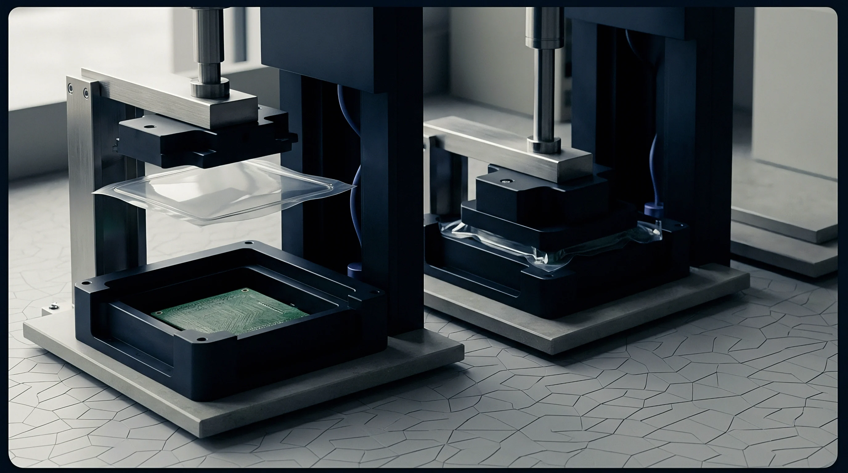
Reconciliation rules identify physical deviations between OEM design specifications and factory laminate inventory. Bring-up stalls when incoming IPC-2581 stack-up files fail to align with locally stocked thickness increments. Software reconciles these differences through pre-configured substitution matrices that recalculate pressed prepreg thickness based on surrounding copper weight, resin flow rates, and lamination pressure.
Automated Stack-Up Reconciliation Rules
The reconciliation engine enforces strict boundary conditions set by the engineering team. When an exact material match is missing from inventory, the engine evaluates candidates using a hierarchical scoring function that weighs dielectric constant delta, thermal expansion matching, glass transition temperature, and total stack height variation ~ accounting for how prepreg flows into trace voids and shifts final geometry.
- Resin Starvation occurs when inner-layer copper filling depletes prepreg resin volume, creating structural micro-cavities along trace edges.
- Impedance Mismatch arises when substituted core laminates shift propagation velocity beyond timing closure thresholds.
- Z-Axis Delamination follows CTE mismatches between unaligned prepreg systems during multiple reflow passes.
- Differential Skew develops when asymmetric glass weave patterns create phase velocity variations between paired conductors.
Automated checks flag physical inconsistencies before fabricators can select unapproved core combinations. If a factory attempts to merge laminates from different material families with unaligned glass transition temperatures, the verification engine rejects the proposed stack-up prior to lamination trials.
IPC-4101E specification sheet compliance guarantees thermal endurance but does not enforce high-frequency dielectric constant uniformity across different lamination lots.
Shop-floor material substitution may yield identical total board thickness, but matching nominal height does not satisfy purchase order requirements without explicit engineering review of signal parameters.

Friction
Secondary bring-up introduces substantial overhead when CAD data transfer lacks automated verification. Manual verification forces engineers to cross-check fabrication drawings, IPC-2581 material declarations, and lamination parameters line by line ~ consuming engineering hours and stretching release schedules.
Commercial Comparison of Verification Workflows
Automating dielectric verification streamlines design transfer, cutting non-recurring engineering costs and accelerating time to market. Instead of spending days on manual line-item checks, automated IPC-2581 scripts process stack-up modifications instantly, recalculating impedance and dielectric tolerances across thousands of nets in seconds.
| Workflow Stage | Manual Verification Hours | Automated Verification Hours | Engineering Cost Delta ($) | Schedule Delay (Days) |
|---|---|---|---|---|
| Data Extraction and Parsing | 12 | 0.1 | -1,785.00 | 2.0 |
| Material Equivalency Check | 16 | 0.2 | -2,370.00 | 3.0 |
| Impedance Solver Recalculation | 24 | 0.5 | -3,525.00 | 4.0 |
| CAM Tooling File Generation | 8 | 0.2 | -1,170.00 | 1.0 |
| Total Bring-Up Impact | 60 | 1.0 | -8,850.00 | 10.0 |
Decision Checklist for Secondary Factory Bring-Up Sign-Off
Engineering managers use structured checklists during secondary factory integration to ensure technical completeness before approving volume production runs.
- Schema Integrity Audit verifies that the incoming IPC-2581 package contains complete copper weight and laminate property fields.
- Material Equivalency Mapping correlates preferred secondary vendor laminates against primary design permittivity tolerances.
- Solvers Verification Loop triggers automated 2D field recalculations for all controlled impedance nets upon stack-up modification.
- CAM Rule Export translates verified stack-up parameters directly into secondary factory panelization and etching tooling systems.
Manual review of multi-layer laminate substitutions introduces human error at every copper thickness boundary.
Automated stack-up verification costs less than a single scrapped lamination run.
Audit
Formal qualification sign-off forms a binding record that ties the fabricator to verified build parameters. Automated stack-up verification generates cryptographic receipts containing complete laminate specifications, impedance solver outputs, and timestamped verification logs. Attached directly to the purchase order, these records establish clear quality benchmarks.
Design Transfer Governance and Ownership Boundaries
A clear division of responsibility between OEM design teams and contract manufacturers prevents disputes during volume production. The OEM retains ownership of netlist intent and impedance specifications, while the fabricator remains responsible for lamination tolerances and chemical etch precision. Comprehensive audit logs and IPC-2581 validation reports document every approved material substitution, settling manufacturing disputes and leaving no room for unapproved shop-floor modifications.
Verification tools embed cryptographic hashes of approved dielectric stack-ups into the final CAM package, ensuring shop-floor drilling and lamination operators process only validated configurations.