Managing Silicon Stepping Discrepancies across Distributed Manufacturing Facilities
Managing distributed silicon steppings requires dynamic firmware stepping detection, fixture speed derating, and contractually enforced reel lot segregation.


Mask
Reels arrive at incoming receiving docks with identical top-side laser markings, but the dies inside often tell a different physical story. Semiconductor foundries track successive revisions of an integrated circuit using stepping codes. An initial tape-out produces a baseline stepping, typically marked A0.
Minor engineering changes touch only the upper metal routing layers to clean up interconnect flaws or timing margins, advancing the stepping designation to A1 or A2. When design teams must resolve base-layer defects in the silicon substrate itself, they re-spin the active diffusion, polysilicon, and implant reticles. That overhaul advances the revision code to B0 or C0.
Foundries also split fabrication across separate geographic facilities to balance line capacity or hedge supply chain exposure. Fab A in Hsinchu might run an older A2 stepping on an established line while Fab B in Singapore qualifies a newer B1 stepping on a recently commissioned 300-millimeter line. Both wafer runs enter the supply channel under the exact same commercial part number.
Distributed electronics manufacturing services (EMS) facilities purchase these components through fragmented regional distributors or direct factory allocations. A manufacturing plant in Guadalajara running surface-mount lines receives reels loaded with A2 stepping silicon. Simultaneously, a twin manufacturing plant in Penang receives reels of B1 stepping silicon for the identical sub-assembly.
The physical silicon inside the plastic packaging carries subtle geometrical and electrical variances that standard bill-of-materials management systems completely overlook.
A full reticle re-spin across forty-five mask layers incurs four hundred thousand dollars in fixed re-tooling fees at mature twenty-eight-nanometer planar nodes.
Foundry teams modify mask sets for three distinct commercial and technical objectives:
- Metal-layer jumper engineering changes reroute connections between existing logic blocks to trim parasitic capacitance spikes without modifying underlying transistor diffusions.
- Base-layer reticle replacements reconfigure active silicon implants to eliminate hard functional deadlocks in internal bus arbiters.
- Shrink reticle optical adjustments reduce overall die surface area by three to five percent to harvest additional gross dies per wafer slice.
Downstream, these mask alterations inevitably register on the surface-mount line. Solder ball pitch and package ball-out dimensions remain nominally constant to satisfy IPC-7351 footprint standards. Package thermal resistance values shift slightly when foundries thin down the backing silicon or replace internal epoxy mold compounds to match new thermal dissipation profiles.
Die attach pad thickness changes high-frequency return paths. Trace impedance values on high-speed serial links drift by three to seven ohms when internal bond-wire lengths vary across disparate packaging facilities, degrading high-speed signals before functional testing begins. Solder joint fatigue profiles alter under cyclic thermal loading when internal silicon die volume drops, concentrating localized mechanical stress around the package perimeter.
Line managers observe localized solder fracturing on secondary plant builds during temperature cycling qualifications while primary plant assemblies pass without incident, even though all delivered lots conform fully to published envelope drawings and pinout tables.


Errata
Hardware documentation rarely travels at the velocity of physical manufacturing lots. Silicon vendors publish errata sheets detailing documented anomalies, peripheral bugs, and internal hardware timing violations for each silicon revision. An A0 stepping might carry twenty-eight distinct hardware defects listed in its silicon errata dossier.
The subsequent B0 stepping resolves eighteen of those initial flaws, yet introduces four brand-new regressions inside modified peripheral state machines.

Peripheral Behavioral Shifts across Revisions
Register behavior often changes significantly between steppings. An analog-to-digital converter peripheral in an initial A-step microcontroller may exhibit an offset error exceeding sixteen least significant bits when operated below two point seven volts. The original firmware team wrote a software calibration compensation routine inside the board support package to correct that offset during boot calibration.
The vendor rectifies the internal voltage reference divider in the B-step silicon. The previously mandatory software calibration routine now overcompensates the analog input readings, introducing an artificial twelve-bit measurement skew into the field units produced at the secondary assembly plant. Clock generation blocks show similar sensitivity.
Phase-locked loop lock times vary widely across mask revisions: a firmware bootloader written to poll the lock status register for two hundred microseconds functions reliably on an A1 stepping, but experiences an intermittent lock timeout on a B0 stepping whose charge pump parameters were adjusted to reduce standby current draw. Sleep current leakage drops from twelve microamps to two microamps on newer silicon, while wake-up transition states gain five microseconds of jitter.
| Silicon Stepping | Fabrication Facility | Affected Subsystem | Physical Root Anomaly | Production Failure Mode |
|---|---|---|---|---|
| Revision A1 | Fab 1 Taichung | Direct Memory Access | Arbiter deadlock during concurrent peripheral bursts | Intermittent SPI bus lockup under saturated sensor telemetry |
| Revision A2 | Fab 1 Taichung | Universal Asynchronous Receiver | Baud rate clock divider fractional jitter at 3.3V | Packet framing errors on long automated test bench cables |
| Revision B0 | Fab 2 Singapore | Analog to Digital Converter | Bandgap reference circuit internal trimming shift | Sensor voltage scaling offset in Guadalajara production lots |
| Revision B1 | Fab 3 Dresden | Deep Sleep Power Controller | Brown-out detector comparator hysteresis reduction | Spurious reset trips during rapid battery load transitions |
Tracking micro-architectural revisions across decentralized operations remains a common failure point. Errata tracking mechanisms sit inside central design repositories, detached from enterprise resource planning systems that manage purchasing at factory floors.
- Interrupted peripheral transfers cause direct memory access engines to halt unexpectedly when receiving simultaneous packet bursts across high-speed serial interfaces.
- Clock synchronization drift creates phase mismatches between peripheral buses and external crystal oscillators, corrupting asynchronous communication packets during rapid thermal shifts.
- Internal voltage comparator flutter triggers false brownout reset interrupts during motor driver startup transients, crashing system firmware in specific plant production batches.
Undocumented silicon behavior generates the most acute factory floor crises, since foundries rarely issue errata updates for behavioral deviations that fall within absolute minimum-maximum electrical specification sheets. Internal pull-up resistor values might measure thirty kilo-ohms on Fab A silicon, yet measure fifty kilo-ohms on Fab B silicon due to different gate oxide thickness tolerances across foundries. Firmware running input-debounce routines on slow-rising edges encounters inconsistent edge-detection timings, leaving engineering uncertain whether secondary fab silicon will silently violate internal bus timing constraints once deployed under extreme operational temperatures.


Patch
Unified binary images frequently fail when deployed indiscriminately across decentralized manufacturing plants. A common procurement practice treats all assemblies sharing a top-level assembly number as functionally interchangeable. Factory A flashes Firmware Build 1.0.4 into an Internet of Things module containing A2 stepping silicon.
Factory B flashes that exact same hexadecimal binary image into the identical module populated with B1 stepping silicon. The secondary plant immediately reports a four percent post-programming failure rate at the in-circuit testing cell.

Why Do Mask Steppings Evade Boundary Scan?
Joint Test Action Group boundary scan routines verify continuity, trace shorts, and basic pin toggling. These structural vector sets do not exercise complex internal sequential logic or peripheral register timing relationships. The boundary scan registers connect to the input-output pads, bypassing core logic entirely.
Silicon steppings alter the internal execution pipeline, cache controllers, and bus crossbars while preserving identical pad boundary behavior. A boundary scan infrastructure passes every single board with zero defects, only for functional failures to emerge ten milliseconds later when the on-chip processor attempts to boot from serial peripheral interface flash memory.
A shared firmware binary across silicon revisions succeeds only when the runtime loader queries hardware revision registers before enabling peripheral drivers.
Dynamic hardware abstraction layers resolve this divergence without requiring split firmware binary releases. Modern microcontrollers and application processors incorporate read-only device identification registers. Silicon designers hard-code the stepping number into specialized system registers, such as the ARM Cortex CPUID Base Register or vendor-specific peripheral identification registers like DBGMCU_IDCODE.
Advanced software architectures execute a silicon identification probe during early bootloader initialization, before standard board support package peripheral initialization routines execute.
Dynamic stepping mitigation relies on three sequential firmware architectural structures:
- Identification reading routines poll the low-level silicon stepping registers and store the hardware revision value inside a dedicated internal memory structure before initializing the system clock tree.
- Conditional vector tables redirect driver function pointers to stepping-specific execution routines designed to account for known peripheral anomalies and register offsets.
- Workaround configuration registers alter peripheral clock dividers, DMA burst thresholds, and internal pull-up configurations to normalize hardware performance across heterogeneous manufacturing lots.
Splitting firmware branches per manufacturing facility creates an operational maintenance catastrophe. If Facility A maintains Branch 1.2-A for older silicon and Facility B maintains Branch 1.2-B for newer silicon, field updates over-the-air require dual fleet management infrastructure. If an end customer re-flashes a field device with the incorrect image, the unit bricks instantly.
A single unified binary containing stepping detection logic adds between four and eight kilobytes of compiled code space. Memory footprint expands slightly, yet eliminates distributed production mismatches. Keeping hardware mitigation routines isolated within low-level hardware abstraction layers protects upper-level application logic from silicon errata churn.


Jig
Automated test equipment cells in disparate contract manufacturing facilities exhibit subtle systemic differences that amplify silicon stepping discrepancies. Test engineers develop the initial functional test bench at an engineering headquarters or primary pilot plant, outfitting that station with high-end programmable power supplies, short low-capacitance pogo pin interconnects, and high-bandwidth digital oscilloscopes. The secondary facility replicates the fixture using regional sheet-metal fabricators, lower-cost switching matrices, and longer test harness cabling.
A circuit assembly running A2 stepping silicon demonstrates sufficient drive strength to overcome the extra fixture capacitance. When the secondary plant switches to B1 stepping silicon, where the foundry intentionally reduced pad slew rates to pass electromagnetic compatibility standards, the test fixture fails the units for rise-time violations.
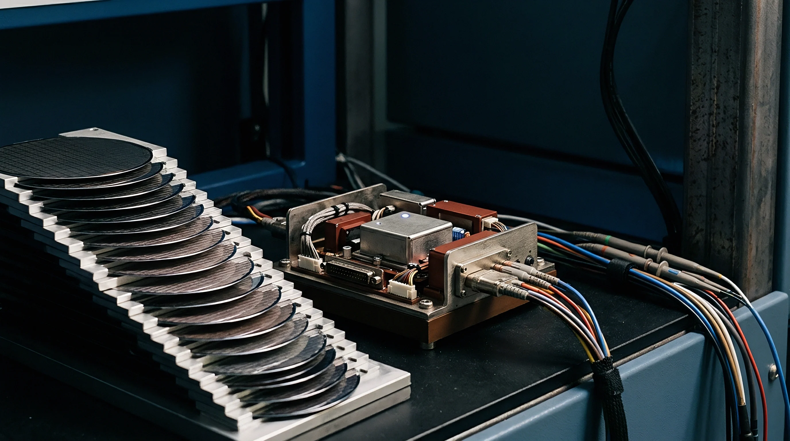
Where Do Secondary Fabs Diverge First?
Test fixture calibration parameters and flashing speeds diverge faster than assembly line mechanical hardware. High-speed flashing algorithms rely on precise timing windows over JTAG or Serial Wire Debug ports. An older silicon revision allows high-voltage flash programming pulses at twelve megahertz.
A newer revision with reduced gate oxide geometry mandates a ten-megahertz flashing speed ceiling to prevent flash memory cell dielectric breakdown. Secondary EMS facilities operating under strict production throughput quotas frequently bypass corporate engineering change notices and crank test bench flashing speeds to maximum limits, causing programming failure rates to surge on the factory floor.
A similar configuration control breakdown occurs in the aviation wiring harness industry, where identical pin crimp terminations fail tensile pull tests when copper wire drawing facilities shift annealing temperatures across regional plants. Electronics assembly suffers that same mechanical and electrical sensitivity when test jigs do not track silicon micro-revisions.
| Facility Location | Station Identifier | Installed Stepping | Flashing Clock (MHz) | Programming Cycle Time (s) | First-Pass Yield (%) |
|---|---|---|---|---|---|
| Pilot Facility Guadalajara | Station Alpha-1 | A2 Stepping | 12.0 | 14.2 | 99.6 |
| Distributed Plant Penang | Station Bravo-1 | A2 Stepping | 12.0 | 14.3 | 99.4 |
| Distributed Plant Penang | Station Bravo-2 | B0 Stepping | 12.0 | 18.9 (Retries) | 91.2 |
| Distributed Plant Penang | Station Bravo-2 | B0 Stepping | 8.0 (Derated) | 19.1 | 99.1 |
| Distributed Plant Rayong | Station Charlie-1 | B1 Stepping | 10.0 | 16.4 | 99.3 |
Consider the production arithmetic of a fifty-thousand-unit monthly production run split equally across two distributed plants. Plant 1 runs A2 silicon with an established test fixture cycle time of sixty seconds per board, achieving a ninety-nine point five percent first-pass yield. Plant 2 receives twenty-five thousand units of B0 silicon.
Station fixtures at Plant 2 experience intermittent flash-verify errors due to a three-microsecond difference in flash write completion times on the newer stepping. The station initiates automatic retry routines, inflating the average test cycle time from sixty seconds to seventy-eight seconds per device.
The operational delay consumes an extra one hundred twenty-five machine hours per month at Plant 2. If the facility operates two eight-hour shifts over twenty-two working days, that delay equates to zero point seven additional dedicated test stations. Capital expenditure for a high-density in-circuit functional test station ranges from forty thousand to eighty thousand dollars.
If the test engineering team fails to adapt the test fixture scripts to account for the stepping difference, the plant either incurs substantial unbudgeted fixture tooling costs or creates an artificial assembly line bottleneck that strands thirty thousand dollars in work-in-progress inventory per week.
A baseline flashing profile must be qualified across every active silicon stepping before releasing test firmware to distributed production lines.
One-time programmable memory blocks and on-chip electronic fuses introduce irreversible production fallout. Engineers configure boot source pins, security keys, and hardware feature flags by blowing internal polysilicon fuses during final board test. Silicon stepping modifications frequently alter internal fuse programming voltage requirements.
Stepping A2 requires three point three volts on a dedicated programming pin for fifty milliseconds. Stepping B0 reduces the maximum allowable fuse-blowing voltage to two point five volts to protect neighboring fine-pitch logic gates. If a distributed manufacturing plant runs the older fixture test profile with three point three volts on the B0 silicon, the programming sequence punches straight through the internal gate oxide, destroying the main processor die permanently.
Because destructive over-voltage errors occur silently, the unit passes initial power-on, but fails five minutes later during functional communication verification. The assembly ends up in the scrap bin, logged incorrectly as an unrecoverable component soldering failure. The manufacturing facility faces tens of thousands of dollars in unrecoverable scrap costs, and line managers point fingers at contract manufacturing surface-mount quality rather than the unmanaged silicon revision drift.


Dock
Managing distributed production across regional facilities requires rigid change-control discipline at the receiving dock and the purchasing desk. Silicon manufacturers operate under standard industry notification rules defined by JEDEC Standard JESD46. This specification governs Product Change Notifications (PCN).
A component supplier must issue a PCN ninety days prior to shipping revised silicon steppings if the revision impacts the form, fit, or function of the component. The standard leaves substantial room for manufacturer interpretation. If the vendor determines that a base-layer revision corrects an erratum while maintaining pin compatibility and functional envelope performance, they classify the change as a non-major stepping update and ship the new stepping without advance customer approval under the existing ordering part number.

Contractual Control and Part Number Segregation
Electronics brands purchasing components through contract manufacturers must establish direct supplier quality agreements that supersede standard commercial terms. Sourcing agreements must explicitly dictate that all silicon stepping changes require written engineering approval, regardless of the vendor’s internal classification under JESD46 guidelines. Sourcing teams enforce this discipline by mandating specific ordering part numbers or unique customer part numbers for every silicon mask revision.
Standard commercial part numbers group multiple silicon revisions under a single catalog designation. Microchip, STMicroelectronics, and NXP establish specific orderable suffix codes that dictate silicon stepping, packaging fab origin, and tape reel lot designations. If purchasing teams at distributed plants order using only the root commercial part number, regional distributors fulfill orders from available local warehouse stock.
Plant 1 receives aged inventory from a domestic warehouse, while Plant 2 receives newly fabricated lots arriving directly from an overseas foundry. The company must enforce a rigid part numbering policy inside its master product data management system. When a new stepping enters production, the component engineering team releases a new internal part number, forcing new incoming inspection criteria, automated test fixture qualifications, and firmware release updates.
JEDEC Standard JESD46 allows semiconductor manufacturers to ship revised silicon steppings without prior customer consent if the supplier classifies the modification as form, fit, and function neutral.
Warehouse lot traceability serves as the final barrier against unintended component mixing on surface-mount lines. Traceability systems in distributed factories must record the specific silicon die stepping, date code, and wafer lot number printed on component reel barcodes. SMT placement systems verify these attributes against the authorized assembly bill of materials before reel feeders unlock on the pick-and-place gantry.
If a reel containing an unapproved stepping is mounted onto a feeder, the line halts immediately. Mixed-stepping production within a single manufacturing batch creates severe quality control tracking issues. If a field recall occurs six months later due to an unaddressed stepping-specific erratum, the brand cannot isolate affected serial numbers without complete reel-to-board traceability data.
Sourcing contracts must mandate that the factory retains reel-level component lot records linked directly to finished product serial numbers for a minimum of seven years.
The standard procurement agreement shifts all financial liability for non-conforming inventory back to the manufacturing partner when the contract states that the supplier guarantees delivery of the specific silicon mask revision identified in the purchase order schedule, invalidating any unilateral product change allowances otherwise permitted under published vendor distribution guidelines.