Radiated Spurious Emission Suppression Techniques for Modular Systems
Effective radiated spurious suppression for modular hardware demands early PCB ground optimization, seam shielding, and systematic host pre-qualification testing.

Spur
Operating a compact wireless transmitter inside an enclosure inevitably produces electromagnetic fields outside the fundamental carrier frequency. High-frequency digital clocks, switching converters, and non-linear semiconductor junctions convert conducted ripple into radiated emissions. In a 3-meter semi-anechoic chamber, these unintended spectral lines show up on turntable scans as sharp narrowband spikes or broader envelope peaks.
When antenna elevation sweeps from 1 to 4 meters pick up these field strength violations, host integrators usually have to halt their market filings.
Energy coupling happens when internal board geometries convert differential mode currents into common mode currents. That common mode energy then drives attached wiring harnesses and metal enclosures, effectively turning passive structural parts into efficient radiating antennas. Suppressing these emissions requires isolation right at the printed circuit board boundary before fields reach external structural elements.
Physics of Unintended Radiated Energy
Non-linear switching transitions in onboard voltage regulators produce high-order harmonics extending far into the gigahertz range. When a transceiver shifts into high-power digital modulation, the power supply rails see transient current draw at both the symbol rate and the clock frequency. If local energy storage isn’t sufficient, the resulting voltage dips generate sideband harmonics around the carrier that exit through dielectric gaps, chassis seams, and connected data buses.
Conducted currents convert to radiated fields via mutual inductive and capacitive coupling. Traces routed without immediate parallel return paths create large differential loop areas, driving up radiated field intensity in proportion to the square of the frequency. At the same time, parasitic capacitance between IC lead frames and nearby shielding allows common mode displacement currents to flow directly into the system ground structure.
| Regulatory Regime | Standard Reference | Frequency Range | Field Strength or Power Limit | Detector / Bandwidth Settings |
|---|---|---|---|---|
| United States (FCC) | FCC Part 15.247 / 15.209 | 30 MHz to 10th Harmonic | 54 dBµV/m at 3m (Above 960 MHz) | Average Detector / 1 MHz RBW |
| European Union (ETSI) | ETSI EN 300 328 Clause 4.3.2.11 | 1 GHz to 12.75 GHz | -30 dBm Effective Isotropically Radiated Power | Peak Detector / 1 MHz RBW |
| Japan (MIC) | Radio Law Article 38-24 | 30 MHz to 26 GHz | 2.5 µW / MHz (-26 dBm/MHz) | RMS Detector / 1 MHz RBW |
| China (SRRC) | GB/T 9254.1 / Radio Type Approval | 30 MHz to 6 GHz | -30 dBm ERP (1 GHz to 40 GHz) | Peak/Average / 100 kHz – 1 MHz RBW |

Measurement Standards across Global Regimes
Test methodologies dictate how raw emission profiles translate to pass or fail outcomes. The Federal Communications Commission evaluates field strength in decibels relative to one microvolt per meter at 3 meters. By contrast, European Telecommunications Standards Institute rules measure absolute radiated power via the substitution method, reporting values in decibels relative to one milliwatt.
When margins are tight, subtle discrepancies between peak detector scans and average measurement limits often trigger unexpected compliance failures.
Field strength measurements conducted at a 3-meter distance under FCC Part 15.209 limits require radiated emissions above 960 MHz to remain below 54 dBµV/m when using an average detector with a 1 MHz resolution bandwidth.
Minor variations in laboratory procedures can alter observed noise margins significantly. A product that easily satisfies CISPR 32 quasi-peak limits below 1 GHz might still fail ETSI peak checks above 1 GHz because of transient digital clock harmonics. Pinpointing the physical source of each emission line requires systematic suppression early in the layout phase.
The central difficulty is ensuring board-level decoupling suppresses third-harmonic energy without degrading power conversion efficiency across temperature extremes.


Stackup
Multi-layer PCB design is the primary defense against electromagnetic field leakage. Running an unbroken ground reference plane right next to high-speed signal routes keeps current loop areas small. Outer-layer microstrip lines tend to create unconfined fields that readily couple into nearby chassis components, whereas buried striplines sandwiched between solid reference planes keep electric and magnetic fields contained within the dielectric.
Ground plane discontinuities force return currents to detour around slots, turning those gaps into effective slot antennas on the board itself. Similarly, signal vias that pass through reference planes without adjacent ground return vias create localized inductive spikes. These impedance shifts generate common mode noise voltages between different functional blocks on the board.

Ground Plane Continuity and via Placement
Low-impedance return paths depend on uninterrupted copper planes beneath high-speed traces. Splitting planes to separate analog and digital grounds often backfires if signal traces cross that boundary, expanding the loop area and driving high-frequency common mode currents into attached cables and structural metal.
Ground stitching vias between top and bottom fills require careful geometric spacing. Placing stitching vias along plane boundaries suppresses edge-radiation effects, and keeping via spacing tighter than one-twentieth of the target harmonic wavelength prevents fields from leaking through the edge dielectric.
- Stitching Via Fences surrounding high-frequency trace routes contain lateral field spreading within the dielectric layer.
- Continuous Reference Layers situated directly below RF trace networks preserve characteristic impedance and suppress return loop areas.
- Power Plane Decoupling Arrays using low equivalent series inductance capacitors direct high-frequency noise to ground locally.
- Embedded Stripline Construction shields sensitive clock signals by routing them between two continuous ground reference planes.

Power Network Decoupling and Filtering
Switching regulators generate broadband conducted noise that easily spreads across power distribution networks. Placing ceramic decoupling capacitors directly at IC power pins sinks ripple current locally. Staggering capacitor values targets distinct frequency bands by taking advantage of their differing self-resonant characteristics.
Series ferrite beads on supply lines attenuate residual high-frequency noise. Selecting the right ferrite means balancing its impedance profile at target harmonic frequencies against DC resistance limits to avoid thermal issues.
Maintaining solid ground plane coverage eliminates open return loop paths.


Aperture
Physical openings in an enclosure act as secondary radiators for internal high-frequency noise. Unshielded seam joints, display windows, and status LED ports allow internal cavity fields to escape as electromagnetic radiation. If an internal noise frequency aligns with the physical dimensions of a slot, that opening behaves like a resonant slot antenna.
Flexible flat cables running to display modules or sensor arrays pose significant common mode radiation risks. Unshielded ribbon cables pick up high-frequency clock harmonics and carry them past the main chassis shielding, bypassing housing attenuation altogether.

Chassis Seams and Structural Slots
Overlapping sheet metal joints create linear slots along chassis seams. Slot length, rather than total area, dictates radiation efficiency: a narrow seam that measures half a wavelength at an internal clock frequency radiates efficiently even if the physical gap is under a millimeter wide.
Installing conductive gaskets or spring fingers along structural seams preserves continuous electrical contact across mating panels. For reliable suppression over full operating temperature ranges, low-resistance contact must be maintained without compromising environmental seals.
Unsealed structural seams exceeding one-twentieth of a harmonic wavelength act as efficient slot antennas, turning internal circuit noise into external radiated emissions.

Cable Shielding and System Interconnects
Wiring harnesses that cross enclosure boundaries require thorough common mode filtering. Shielded cables with 360-degree bonding to the chassis wall prevent noise currents from riding the outer conductor surface, whereas pigtail ground connections introduce enough inductance to destroy shield effectiveness at gigahertz frequencies.
Board-to-board connectors placed near enclosure openings often couple fields directly into internal wiring. Placing common mode chokes on connector signal lines suppresses high-frequency noise before signals escape the shielded volume.
- Conductive Gasket Striping compresses along housing joints to bridge mechanical gaps and eliminate resonant slot antennas.
- Peripheral Cable Bonding secures 360-degree shield contact directly to chassis metal to prevent common mode current propagation.
- Absorbing Sheet Layering lines internal plastic housing walls to convert near-field electromagnetic energy into thermal energy.
- Filtered Interface Connectors integrate surface-mount transient suppression and ferrite elements directly within the physical jack housing.
Choosing improper gasket compression densities can distort structural panels and cause unexpected harmonic radiation in the field.

Scope
Integrating a modularly certified radio transceiver does not guarantee final product compliance. Modular approvals only evaluate radio performance under unshielded, standalone conditions on an evaluation board. Placing that module inside a custom enclosure alongside power supplies and high-speed digital buses alters the entire radiated spectrum.
Host integration requires thorough re-verification of radiated spurious emissions. Regulatory bodies hold the host manufacturer responsible for compliance of the complete assembly, regardless of pre-certified wireless components.

Do Host Enclosures Shift Modular Compliance Boundaries?
Host enclosures alter both the radiation pattern and near-field coupling of pre-approved modules. Housing a module in plastic shifts antenna resonance, changing center frequencies and often elevating harmonic emissions. Metal enclosures contain internal fields better, but they introduce cavity resonances that can amplify specific spurious bands.
When integration alters original grant conditions, regulatory bodies require host evaluation through Class II Permissive Changes or updated technical construction files. Altering antenna trace layouts, swapping antenna types, or reducing separation distances voids standalone modular grant coverage.
- Review original modular grant documentation to establish baseline spurious emission levels and certified antenna constraints.
- Mount the module within the final host enclosure with all peripheral subsystem cables and power supplies installed.
- Execute preliminary radiated emissions pre-scans across all active operating bands inside an anechoic chamber.
- Compare observed spurious energy against standalone grant limits to identify host-induced noise contributions.
- File a Class II Permissive Change or update the Technical Construction File based on observed regulatory headroom.

Permissive Changes and Assessment Re-Evaluation
FCC rules define specific permissive change routes based on emission variations. A Class I Permissive Change applies if circuit modifications do not degrade radiated spurious levels. A Class II Permissive Change requires formal lab data submission when the host enclosure introduces measurable spurious increases while remaining under legal limits.
Federal Communications Commission guidance KDB 996369 D04 mandates that host manufacturers perform radiated spurious testing on co-located modules to verify no new emission lines exceed regulatory limits.
European compliance falls under the Radio Equipment Directive framework. When integrating certified modules into host equipment, integrators must back their Declaration of Conformity with updated assessment records.
Standalone modular grants do not guarantee host compliance, as host power converter coupling can generate non-compliant third-harmonic emissions during laboratory testing.


Campaign
An efficient test plan separates diagnostic pre-qualification from formal regulatory testing. Running diagnostic scans early in development catches suppression gaps while mechanical and PCB changes are still inexpensive; relying entirely on final compliance testing adds major schedule risk.
Maximizing chamber time requires solid preparation. Configuring dedicated test firmware to force continuous transmitter modulation across low, middle, and high channels speeds up lab throughput significantly.
Pre-Qualification Screening Protocols
Near-field benchtop scans isolate radiating traces long before entering a semi-anechoic chamber. Magnetic field probes locate IC clock emissions, electric field probes highlight noisy cable interfaces, and surface current mapping points to optimal locations for ferrite elements and shielding cans.
Comparative pre-scans in small chambers validate suppression fixes against baseline measurements. Testing PCB stackup options during pre-qualification ensures proper filter selection before committing to final tooling.
- Excessive Near-Field Coupling around display flex connectors indicates inadequate ground return paths along high-speed signal routes.
- Broadband Floor Elevation across sub-gigahertz bands signals switching regulator noise spreading into system ground structures.
- Localized Harmonic Peaks appearing exclusively during modulation reveal power amplifier power supply instability.
- Directional Emission Asymmetry during turntable rotation indicates chassis slot antenna formation along enclosure seams.

Chamber Diagnostics and Sample Provisioning
Formal qualification calls for multiple identical test units running specialized test firmware. The control software needs to support fixed-frequency transmission, adjustable duty cycles, and unmodulated carrier modes, since testing under standard burst modes risks missing intermittent spurious spikes.
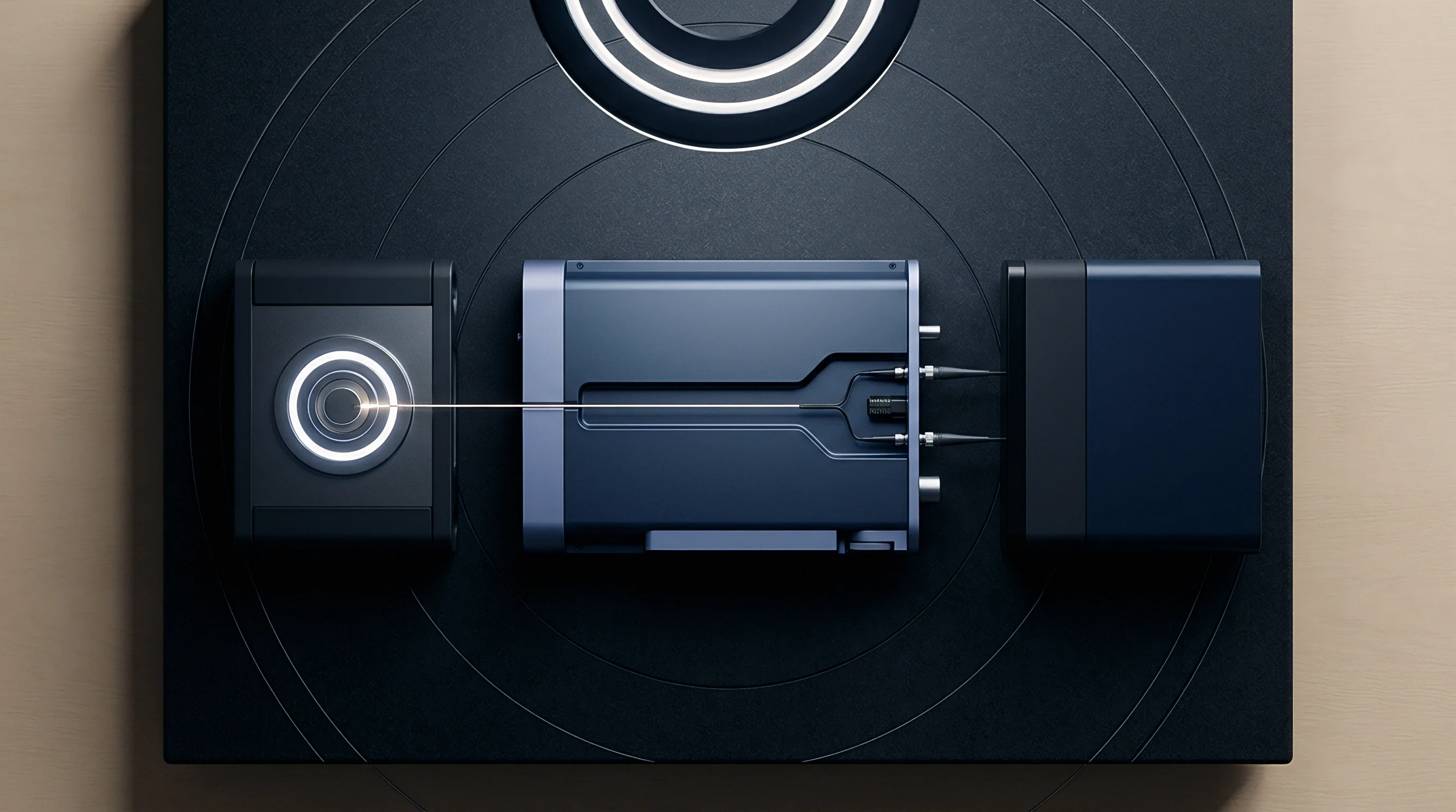
Sample preparation involves modifying host units to expose control interfaces without creating RF leakage paths. Using fiber-optic control lines prevents external test cabling from skewing radiated chamber measurements.
Under ISO/IEC 17025 accreditation guidelines, all spurious emission test equipment must maintain traceable calibration within twelve-month intervals.

Outlay
Spurious suppression carries both direct design costs and schedule commitments. Board respins, shielding tooling changes, and extra chamber time add up fast when compliance failures occur late in development. Investing early in robust suppression minimizes re-certification overhead down the line.
Commercial planning means mapping out country-specific submission routes early. Synchronizing test campaigns avoids duplicate lab fees and reduces launch delays across export markets.

Financial Arithmetic of Retesting versus Mitigation
Failing a chamber run costs far more than just hourly lab fees. Re-tooling a PCB takes engineering time and fab lead time, while retesting delays product shipments and eats into revenue.
Adding thorough suppression in the initial hardware design raises the bill of materials slightly. Extra ground vias, shielding cans, and ferrite beads add modest per-unit costs compared to the hit from a delayed commercial launch.
| Suppression Strategy | BOM Impact (USD) | Tooling / NRE (USD) | Testing Overhead | Schedule Impact |
|---|---|---|---|---|
| Initial Board Optimization | 0.15 to 0.45 | 1,200 to 3,500 | Baseline Pre-scan | Zero Delay |
| Chassis Shielding Gaskets | 0.30 to 1.10 | 2,500 to 8,000 | Seam Leakage Re-scan | 1 to 2 Weeks |
| Board Respin (Late Phase) | 0.00 to 0.50 | 5,000 to 15,000 | Full Retest Cycle | 4 to 8 Weeks |
| Class II Permissive Filing | N/A | 1,500 to 4,000 | Radiated Spurious Only | 2 to 4 Weeks |
| Full Host Re-Certification | N/A | 8,000 to 22,000 | Complete Chamber Suite | 6 to 12 Weeks |

Sequencing Global Regulatory Filings
Optimizing filing sequences relies on mutual acceptance of test reports between jurisdictions. An FCC grant and CE test report based on 3-meter chamber data form the baseline evidence for secondary filings, as regulators in Japan, South Korea, and Brazil accept accredited lab data formatted to local standards.
Sequential regulatory filings leveraging core FCC and CE radiated spurious test reports reduce regional type-approval fees by up to 60 percent.
Securing major market approvals first helps fund downstream regional certifications. Careful management of lab schedules and paperwork keeps global access moving without unexpected regulatory hiccups.
Global rollout schedules depend on establishing solid spurious suppression at the board level during initial layout. Aligning chamber bookings with firmware milestones prevents wasted lab time while debugging harmonic noise. Host integration risk drops when teams evaluate pre-certified modules as RF components requiring full system-level validation, turning complex international type approvals into manageable project steps.