Meaning
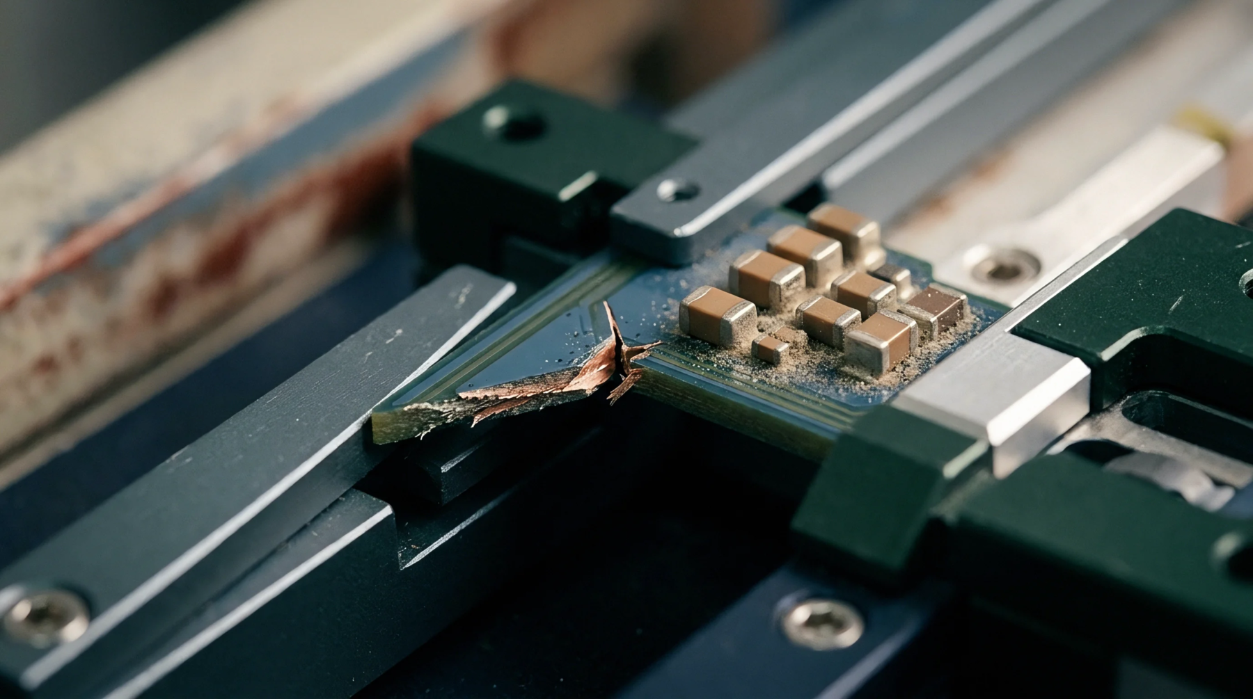
An unpopulated substrate features conductive pathways etched from copper sheets laminated onto a non-conductive base. Before components are attached, a bare printed circuit provides the physical structure and electrical connections for an electronic device. Multi-layer designs employ internal pathways to route signal lines through complex arrays.
Mechanical drill holes and plated vias establish the pathways between layers.
Substrate Composition
Fiberglass reinforced epoxy resin acts as the standard structural core for rigid boards. When selecting the material, a designer evaluates the glass transition temperature to ensure thermal stability during soldering. Copper foil is bonded to this core under heat and pressure.
This metallic layer is then patterned through photolithography.
Electrical Testing
Verifying the integrity of every connection ensures the board is free of manufacturing defects. During this verification stage, a bare printed circuit undergoes fixtureless flying probe testing or bed-of-nails testing to detect open circuits and short circuits. Automatic optical inspection also checks the trace widths and pad spacing against the original files.
This step guarantees that only fault-free boards proceed to the component mounting phase. High-voltage insulation tests check the resistance between adjacent traces to prevent dielectric breakdown in service.
Assembly Integration
Solder mask is applied to protect the copper traces from oxidation and to prevent accidental solder bridging. Solderable surface finishes, such as organic solderability preservatives or electroless nickel immersion gold, are deposited on the exposed pads. This preparation prepares the board for the automatic pick-and-place process.
Proper pad finish selection is necessary to secure reliable solder joints.