In Circuit Testing Physical Node Access Protocols for Modified Assemblies
Reworked PCBA node access requires mechanical probe relief, netlist reconciliation, and target re-mapping before executing in-circuit tests.

Disruption
Modifications to multi-layer printed circuit boards change physical land geometries and disrupt automated factory inspection routines. When engineering change orders (ECOs) arrive after layout sign-off, technicians routinely apply post-fabrication fixes directly onto assembled boards. These physical interventions ~ manual trace cuts, enamel wire jumpers, dead-bugged surface-mount components, and pull-up resistors soldered across exposed pins ~ restore functional performance in prototype units, but they dismantle the mechanical and electrical assumptions governing in-circuit test (ICT) node access.
Bed-of-nails ICT systems rely on exact spatial predictability. Standard fixtures use spring-loaded pogo pins aligned to hit flat copper test pads measuring between 0.6 mm and 1.0 mm in diameter, positioned on a 1.27 mm or 2.54 mm grid across the bottom surface of the printed circuit board assembly (PCBA). When an ECO introduces wire jumpers or shifts surface passives, that flat target area becomes an irregular three-dimensional profile.
Pogo pins designed for flat target pads hit round wire insulation, solder mounds, or empty board space, causing pin deflections, mechanical damage, and high false-fail rates during automated manufacturing testing.

Engineering Alterations in High Density Circuitry
Dense board layouts lose physical testability when surface jumper wires overlay dedicated copper pads. Solder height accumulates quickly: a 30 AWG kynar wire jumper soldered directly to a component pad creates a solder mound rising 0.8 mm to 1.5 mm above the board surface. Standard pogo plungers contacting this irregular solder geometry experience off-axis vector forces that push the spring pin sideways, scraping conductive solder onto adjacent signal traces or bending the plunger stem within its mounting receptacle.
Trace cuts introduce equal diagnostic disruption. Cutting a surface trace with a scalpel breaks one continuous electrical node into two distinct electrical nets, yet the original test program still treats the surviving target pad as representative of the entire trace. Because test algorithms evaluate node impedance against unmodified schematic netlists, short- and open-circuit checks produce invalid diagnostic data, triggering phantom isolation failures that halt automated assembly lines.
Mechanical Obstructions on Bed of Nails Fixtures
Spring-loaded plunger arrays require flat, smooth landing zones across exposed component interconnects. Standard test fixture press plates pull the circuit board down using vacuum seals or mechanical pusher rods, driving the board against hundreds of rigid spring probes under high spring force ~ typically 1.5 to 2.8 Newtons of force at full travel. When a jumper wire sits directly beneath a pusher rod or within the travel path of an unadjusted pogo pin, compressive force crushes the jumper wire insulation, shorting internal wire strands against adjacent components.
Physical changes on assembled circuit boards invalidate established spring-probe contact patterns and false-fail rates increase immediately.
Dead-bugged components present even greater physical interference. When fixture pushers exert vertical force directly onto an upside-down integrated circuit suspended by fine copper wires, solder mask bridges can block probe contact while structural strain ruptures the manual solder joint underneath. These ruptured joints often maintain contact during initial vacuum actuation, only to open later under thermal stress in the field.
Operating modified circuit boards on unadjusted fixtures bends target pins, destroys dead-bugged solder joints, and sends misdiagnosed assemblies into scrap bins.

Target
Precise electrical contact depends on maintaining strict mechanical tolerances between spring pins and board copper features. Standard ICT land patterns demand a minimum target pad diameter of 0.8 mm for reliable contact using standard 100-mil pogo probes. When rework or physical board revisions force components into former test point keep-out zones, test target areas shrink or vanish entirely.
Retaining physical node access on modified assemblies demands strict re-mapping of target geometry, pin tip selection, and mechanical clearance envelopes around post-assembly modifications.
Shifting a surface-mount passive component by 0.5 mm to clear a newly routed wire jump reduces the clearance distance between the component body and adjacent test targets. If the keep-out distance drops below 0.35 mm, standard probe barrels rub against component bodies, introducing parasitic capacitive coupling and mechanical alignment errors.
Physical Keep out Volumes for Surface Wiring
Adding discrete jumper leads creates three-dimensional vertical clearance zones that deflect standard pogo plungers. To prevent physical contact between spring probes and surface wire runs, test engineers establish three-dimensional keep-out volumes around every manual wire installation. A standard wire jumper installation requires a clear physical radius of at least 1.0 mm around the entire wire path, extending 2.0 mm vertically above the board plane.
| Modification Type | Nominal Target Diameter | Minimum Keep-Out Clearance | Maximum Allowable Height | Recommended Probe Tip Geometry |
|---|---|---|---|---|
| Unmodified Standard Pad | 0.80 mm to 1.00 mm | 0.40 mm radius | 0.15 mm (Pad height) | 90-Degree Spear / Serrated Crown |
| Relocated Test Pad | 0.50 mm to 0.65 mm | 0.25 mm radius | 0.15 mm (Pad height) | Micro-Needle / Sharp Chisel |
| 30 AWG Jumper Wire Termination | 1.20 mm (Solder mound) | 1.00 mm radius | 1.80 mm above PCB | 7-Point Crown / Tulip Head |
| Cut Trace / Split Net Node | 0.40 mm (Exposed copper) | 0.50 mm radius | 0.10 mm (Trace depth) | Flat Point / Self-Cleaning Chisel |
| Dead-Bugged Component Lead | 0.35 mm (Solder bead) | 0.80 mm radius | 2.50 mm above PCB | Concave Cup / Spherical Radius |
Probe Tip Selection and Alignment Criteria
Chisel heads puncture severe oxide layers on unwashed solder pads, whereas crown plungers center themselves on rounded lead spheres. Because non-conductive flux residue builds up thick insulating coatings over hand-soldered target pads, choosing the correct probe tip shape determines whether an ICT system achieves low-resistance contact without slipping off the target profile.
When probing hand-soldered ECO pads, flux residue accumulation presents a major electrical barrier. Smooth spherical or flat probe plungers skid off wire leads or fail to pierce this insulating layer, producing false open-circuit readings. Serrated crown tips or self-cleaning chisel points concentrate spring force onto sharp points, cutting through flux films to achieve reliable metal-to-metal contact.
Target alignment drift further limits physical access accuracy. Board substrate thermal expansion during soldering, combined with mechanical tolerances in fixture locator pins, produces target positioning variations up to ±0.12 mm across a 300 mm board span. When target pad diameters decrease below 0.6 mm following ECO modifications, optical alignment or flying probe systems become necessary to compensate for physical target position shifts.
Target diameters below 0.6 mm demand optical probe centering when board substrate expansion exceeds 0.08 percent.
List of failure modes during physical probe engagement on modified nodes:
- Plunger Stem Deflection occurring when a spring pin strikes an angled solder surface on a jumper wire termination, causing the plunger to bend laterally and short against neighboring component pins.
- Flux Insulation Open resulting from manual rosin residue forming an insulating barrier over hand-soldered target pads that low-force probes fail to pierce.
- Substrate Delamination Strain created when excessive pogo spring pressure concentrates on a reduced target pad area adjacent to a manual trace cut.
- Wire Shearing Failure happening when an un-relieved pusher rod or fixture plate edge pinches an enamel wire jumper against a sharp PCB ground plane edge during vacuum seal pull-down.
- Intermittent Contact Bounce caused by residual mechanical vibration in modified long-stem flying probe needles striking non-planar surface-mount passives.
Smaller target surfaces call for lower spring force plungers to prevent board flexure during multiple fixture actuations.
Fixturing
Adapting dedicated test hardware for updated circuit layouts demands precise mechanical adjustments to pin placement plates. When board modifications alter physical node locations or add surface wiring, fixed bed-of-nails fixtures require mechanical retrofits to prevent physical interference and restore probe access. Alternatively, production lines transition to flying probe testing systems, which replace rigid bed-of-nails plates with programmable robotic test arms.
While flying probes reduce tooling delays, adjusting physical node access protocols on modified assemblies still requires systematic modification of mechanical fixture hardware, optical alignment offsets, and sensor drive signals.
Retrofitting Bed of Nails Plunger Plates
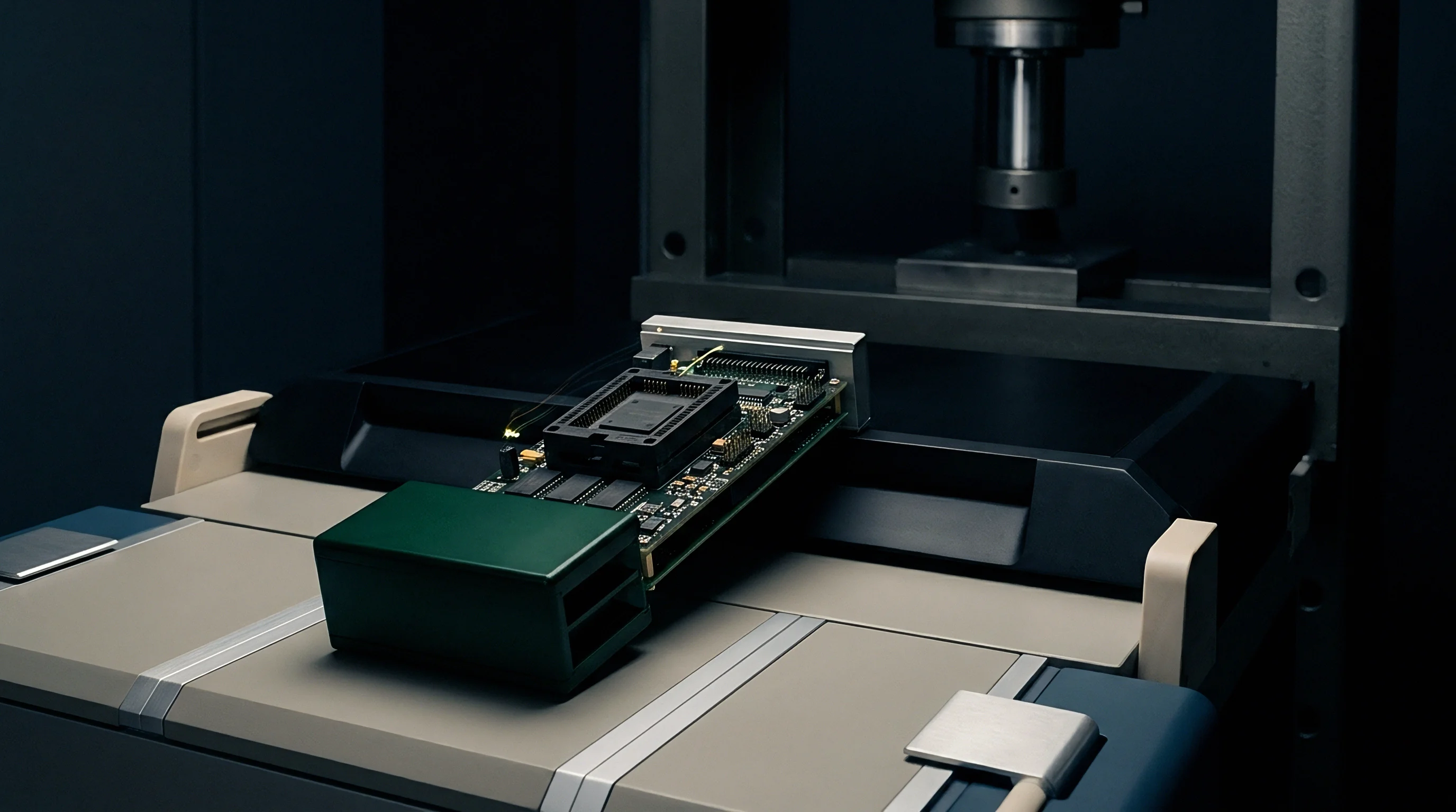
Milling relief pockets into insulating support structures creates room for hand-soldered ECO conductors. Fixture modification starts with removing the top press plate and probe retainer plates from the fixture shell. Technicians transfer updated CAD drill coordinates into a computer numerical control (CNC) milling machine to modify probe plate hole patterns.
- Mount the existing acrylic or G10 probe retainer plate onto a high-precision CNC drill table using primary fixture locating pins for datum reference.
- Mill 3.0 mm relief pockets on the underside of the top push plate directly above newly added jumper wire paths to prevent mechanical crushing during vacuum pull-down.
- Re-drill relocated pogo pin receptacle holes using carbide micro-drills to accommodate shifted target pad positions, maintaining perpendicularity within ±0.02 mm.
- Extract obsolete pogo pin receptacles from abandoned net targets and press insulating acrylic filler plugs into the empty plate apertures.
- Install new spring probe receptacles, wire wrapping individual tail pins to interface matrix boards according to updated pin-to-channel mapping documentation.
- Verify individual pin heights and stroke spring tension across the modified grid using an optical depth micrometer before mounting the fixture back onto the test bench.
Flying Probe Optical Calibration for Relocated Nodes
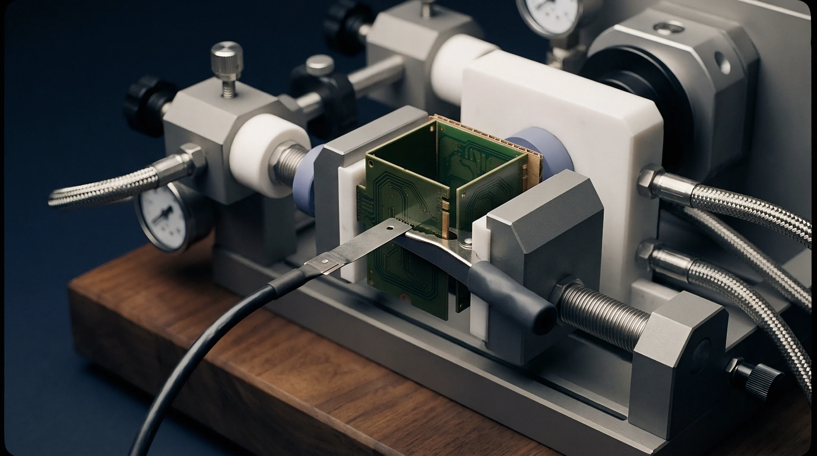
Automated vision systems re-map target coordinates by scanning physical board fiducials against revised Gerber layers. Flying probe systems bypass fixed bed-of-nails hardware by using four to eight independently controlled robotic probes equipped with high-resolution cameras. When evaluating modified assemblies, flying probe systems rely on dynamic optical alignment algorithms to adapt to physical surface variations.
The vision system scans fiducial marks on the modified PCBA, calculating local translation, rotation, and board warp matrices. When a target pad has moved or shrunk due to an ECO rework, the operator updates the test program CAD coordinate file. The flying probe camera scans the target site, detects the precise edge of the modified copper pad, and applies a local displacement offset to the probing coordinate vector.
Because pin force directly alters contact resistance, soft z-axis controls reduce probe tip force to 0.3 Newtons when landing on fragile hand-soldered ECO joints, avoiding damage to delicate wire bridges.
Drill drift and warped top plates stem from client-supplied CAD mismatches as often as tool wear.

Coverage
Mathematical fault isolation models evaluate whether electrical test steps reliably locate short circuits across altered conductive traces. Physical board modifications alter node access, directly degrading test coverage metrics. When an ECO forces the removal of a pogo pin due to mechanical interference, or when a trace cut divides a net into un-probed sub-nets, the overall percentage of detectable manufacturing faults drops.
Quantifying this degradation requires systematic net isolation arithmetic and hybrid fault injection analysis.
Because unprobed nodes mask manufacturing defects, evaluating structural coverage on a modified PCBA requires separating total circuit nodes into fully probed nodes, partially probed split nets, and completely isolated un-probed nodes. The mathematical model calculates fault detection probability based on physical node accessibility and measurement guard conditions.

Quantitative Isolation Models for Split Nets
Splitting a single net into isolated segments alters the admittance matrix used in automated fault diagnostics. Consider a worked mathematical example evaluating node access degradation and fault coverage calculation following an extensive engineering change order on a complex mixed-signal assembly.
State the initial structural conditions and ECO modification parameters:
Assume an assembly containing N = 450 total electrical nodes on a multi-layer board. Prior to modification, the standard ICT bed-of-nails fixture accessed N_accessed = 434 nodes using dedicated 1.0 mm test pads, achieving an initial structural node coverage C_initial of 96.44 percent.
An ECO introduces physical modifications across 12 primary nets. The modification involves cutting 6 trace segments, adding 18 physical wire jumper runs, dead-bugging 2 logic ICs, and inserting 4 discrete 100-ohm series isolation resistors directly into signal paths. Due to spatial crowding and wire overlay interference, 14 existing test pads become physically inaccessible to fixture pogo pins.
The accessible node count drops to N_modified = 420 nodes.
Calculate the modified structural node coverage C_modified:
C_modified = (N_modified / N) 100 = (420 / 450) 100 = 93.33 percent.
The modification creates a direct structural coverage drop of 3.11 percent across the assembly.
Now evaluate signal injection diagnostic thresholds across a split net containing an added 100-ohm series resistor R_series. The test algorithm attempts to detect an analog short circuit to ground (R_short < 2.0 ohms) on the downstream side of the split net (Node B), while probing occurs exclusively at the upstream side (Node A).
The total measured resistance to ground from Node A, R_measured, equals:
R_measured = R_series + R_short + R_contact
Assuming a worst-case contact resistance R_contact of 0.50 ohms across a flux-coated target pad, the measured resistance under a true short condition equals:
R_measured = 100 ohms + 2.0 ohms + 0.50 ohms = 102.50 ohms.
Because standard short-circuit detection thresholds operate with an upper cutoff of R_threshold = 5.0 ohms, the ICT system registers Node A as a normal open net, failing to detect the dead short on Node B. Detecting this fault demands updating the test algorithm to execute guarded low-current resistance measurements across Node A, adjusting short-circuit detection limits to account for known series resistor values inserted by the ECO.
| Modification Scenario | Pre-ECO Net Coverage | Post-ECO Net Coverage | Fault Isolation Capability | Diagnostic Mitigation Protocol |
|---|---|---|---|---|
| Trace Cut without Added Test Point | 100% (Single Net) | 50% (Probed Side Only) | Fails Open Detection on Unprobed Segment | Inject Boundary Scan Vector on Far End |
| Wire Jumper Overlapping Existing Pad | 100% (Direct Pin) | 0% (Pin Removed for Clearance) | Total Loss of Direct Analog ICT | Transition Net to Flying Probe Optical Offset |
| Series Resistor Added in Signal Path | 100% (Low Resistance) | 100% (Impedance Shifted) | Masks Downstream Shorts to Ground | Apply Guarded Resistance Threshold Delta |
| Dead-Bugged Logic IC Integration | 100% (Standard IC) | 25% (Pin Access Lost) | Inability to Verify Internal Gate Switching | Execute Hybrid Functional Cluster Test Step |
Can Boundary Scan Maintain Isolation When Jumpers Obscure Physical Pads?
Digital boundary-scan architecture injects bit vectors through integrated circuit boundary cells to check net continuity without surface pins. Combining IEEE 1149.1 boundary-scan protocols with physical ICT access restores fault detection coverage on modified assemblies without requiring physical probe contact on every net segment.
Per IPC-9261 standards, unprobed nodes on modified assemblies require written engineering authorization detailing residual fault risks before batch release.
When physical jumpers obscure surface test pads, boundary scan shift registers deliver digital stimulus signals down the modified traces. The receiving IC boundary cell captures the bit pattern, confirming electrical continuity across cut traces and manual wire jumpers. Hybrid test systems combine boundary-scan digital coverage with selective flying probe analog measurements, recovering overall structural defect coverage to levels above 98 percent on complex modified boards.
Whether boundary-scan registers can reliably detect high-resistance cold solder joints beneath manual jumper wire terminations remains a subject of active field research.
Handover
Reconciling engineering change records between design teams and contract manufacturers ensures physical test programs match physical hardware updates. When an ECO alters board trace routing or component placement, manufacturing documentation packages must update immediately. A failure in file transfer protocols creates dangerous mismatches where automated test fixtures attempt to probe non-existent pads or apply voltage vectors to newly grounded traces.
Because net reconciliation prevents false failures, maintaining synchronized physical node access requires precise software file overlays, netlist reconciliation tools, and standardized manufacturing change dossiers.

Engineering Change Synchronization across File Formats
Discrepancies between schematic netlists and physical board layouts trigger immediate false opens during automated test generation. Modern electronics assembly relies on IPC-2581 or Gerber X2 file formats to transfer digital manufacturing definitions from CAD software to factory test generation programs. When an offline rework operation occurs, design engineers must update CAD source schematics and PCB layout databases simultaneously.
Unmatched netlist changes disrupt test vectors. Test generation software imports the revised IPC-2581 file and executes an automated netlist comparison against the original test program. The comparison algorithm highlights altered net topologies, newly created split nets, and modified target pad coordinates.
The test engineer reviews these flagged discrepancies, approving software vector modifications before generating updated drill files for fixture modification or updated coordinate scripts for flying probe execution.

Documentation Dossiers for Second Source Production
Transferring modified manufacturing files to an off-site assembly factory demands explicit mechanical drill overlay files. When dual-sourcing or transferring assembly production to a secondary manufacturing facility, the primary design owner must provide a comprehensive design transfer package documenting every physical board alteration.
Always re-run netlist comparison scripts after manual wiring changes before committing fixture modification tooling orders.
Decisions and document items required in an engineering change transfer package for modified assemblies:
- Revised IPC-2581 Fabrication Layer Data incorporating precise mechanical layer definitions of all trace cuts, added copper lands, and altered solder mask openings.
- Mechanical Wire Routing Map detailing wire jumper gauge specifications, insulation material, explicit start-to-finish point landing coordinates, and maximum allowable wire height limits.
- Reconciled CAD Netlist File containing updated net names, split-net naming conventions, inserted passive component values, and modified pin-to-net connectivity matrices.
- Fixture Modification Drill File providing precise micro-drill coordinates, hole diameters, and relief pocket milling depths for bed-of-nails pin plate retrofits.
- Flying Probe Vector Adjustment Script containing visual alignment fiducial changes, soft-landing z-axis pressure settings, and soft-landing probe contact delays.
- Residual Fault Risk Matrix defining specific un-probed net segments, downgraded coverage percentages, and supplemental functional cluster test steps required for quality sign-off.
Under standard ISO 13485 revision clauses, an unverified netlist change invalidates factory quality release sign-offs and transfers full liability for field escapes back to the design owner.

Invoice
Financial accountability for test fixture modifications depends on clear contract definitions of engineering change scope. Modifying physical node access protocols introduces real non-recurring engineering (NRE) costs, fixture material expenses, and manufacturing line cycle-time penalties. Quantifying these financial trade-offs allows product owners to select the most cost-effective integration level when managing ECO updates on active production lines.
Because fixture modification costs add up quickly, choosing between retrofitting an existing bed-of-nails fixture and transitioning to a flying probe test architecture hinges on volume amortisation, unit price impact, and non-recurring engineering labor charges.

Tooling Retrofit Pricing and Engineering Non-Recurring Expenses
Re-drilling acrylic probe plates incurs machine operator hours, replacement pin hardware costs, and test program validation labor. A complete bed-of-nails fixture modification typically requires 12 to 24 engineering hours for netlist re-programming, CNC plate re-milling, and manual pin re-wiring. Material expenses include custom pogo pins, specialized crown tips, wire-wrap receptacles, and replacement top plates.
| Integration Level Scope | Typical Engineering Hours | NRE Material & Tooling Cost | Test Execution Cycle Time Impact | Minimum Volume Break-Even Point |
|---|---|---|---|---|
| Turnkey Contract Manufacturer | 15 to 30 Hours | $2,500 to $5,000 | Zero Increase (Bed-of-Nails Retained) | > 2,500 Units |
| Semi-Custom Integration House | 20 to 45 Hours | $1,800 to $3,500 | +5% to +12% (Hybrid Boundary Scan) | 1,000 to 2,500 Units |
| White-Label Module Vendor | 8 to 16 Hours | $800 to $1,500 | +150% to +300% (Flying Probe Conversion) | < 500 Units |
| In-House OEM Engineering Desk | 30 to 60 Hours | $3,000 to $6,500 | Zero Increase (Custom Fixture Re-Build) | > 5,000 Units |

Amortising Flying Probe Cycle Times against Tooling Costs
High-volume production lines absorb dedicated fixture modification expenses faster than low-volume builds using flying probe systems. While switching a modified assembly from a bed-of-nails fixture to a flying probe system avoids upfront tooling fees and prevents delivery delays, flying probe systems move needles mechanically ~ taking 45 to 120 seconds per board compared to 3 to 8 seconds on a vacuum fixture.
Extra test time directly increases unit costs. On a high-volume manufacturing run of 20,000 units, adding 60 seconds of flying probe test time per board increases total factory machine time by over 330 hours. At standard assembly machine rates of $85 per hour, the cycle-time cost penalty reaches $28,305.
In this high-volume scenario, spending $4,000 in upfront NRE fixture modification fees to retain fast bed-of-nails physical access represents the optimal commercial decision. For prototype or short-run volumes under 500 units, accepting higher flying probe unit test costs avoids expensive fixture re-tooling expenses entirely.
Commercial contracts that explicitly assign probe plate re-drilling and netlist alignment labor to the design owner avoid billing disputes when board alterations delay volume shipment dates.