Meaning
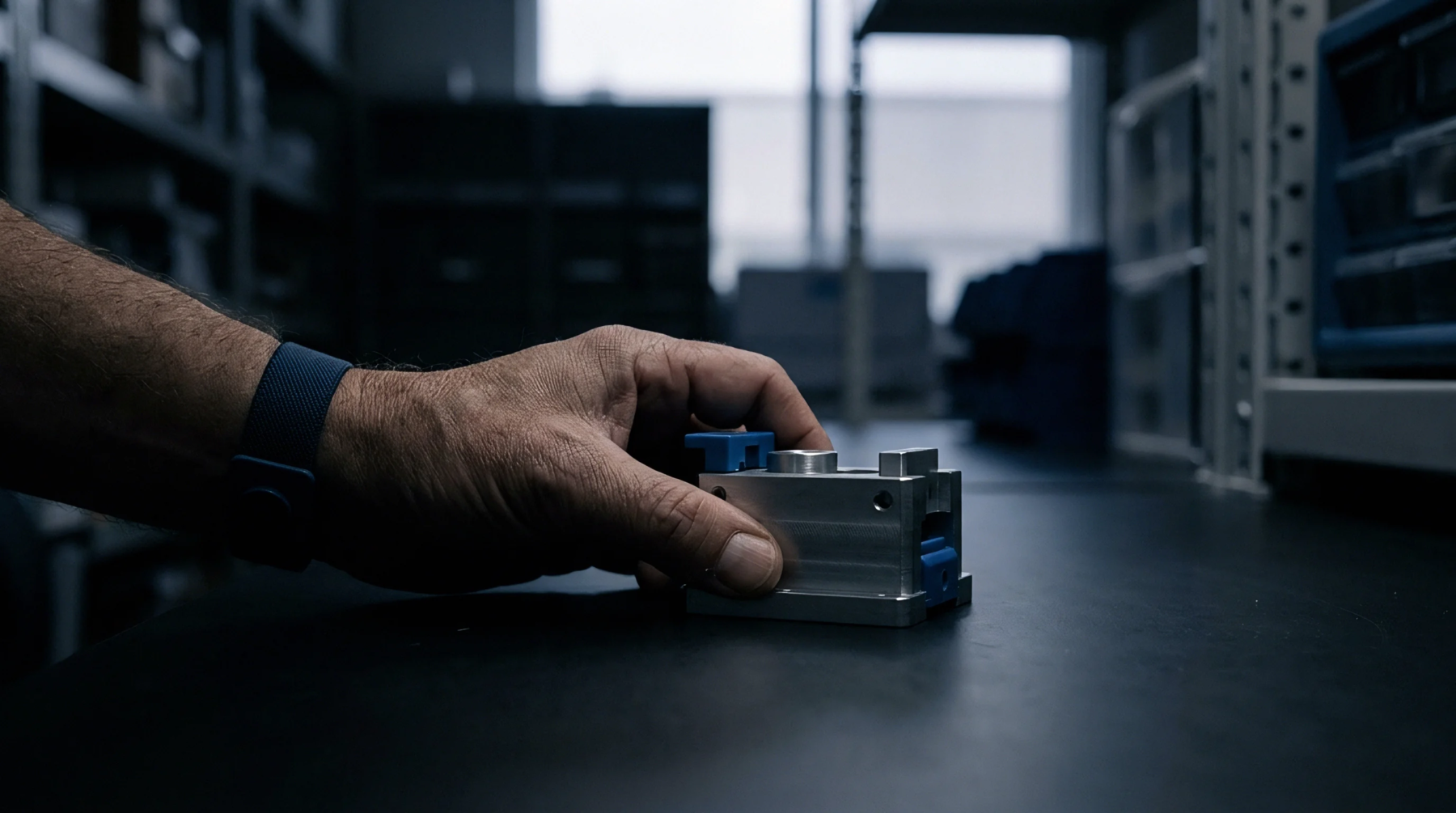
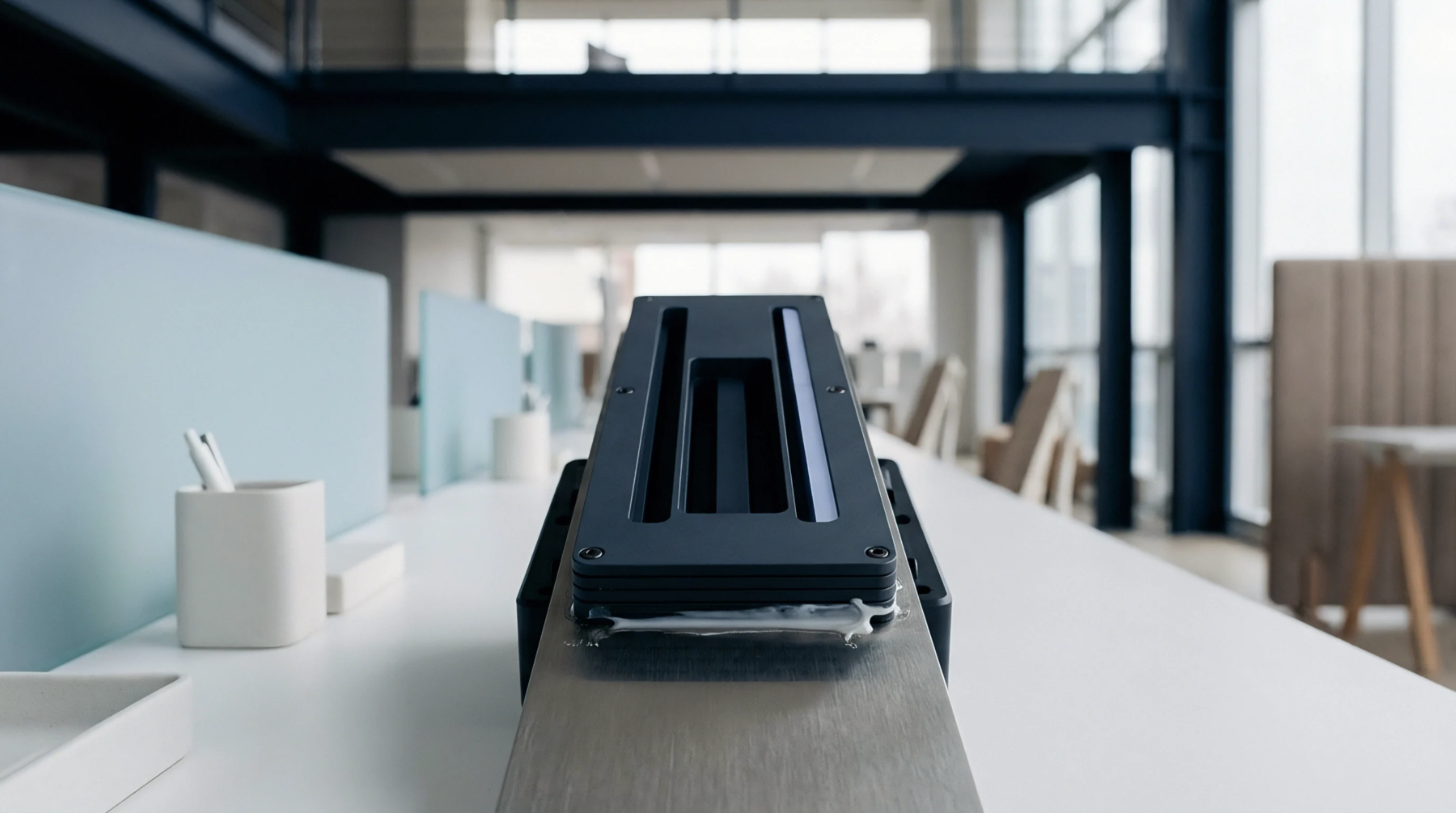
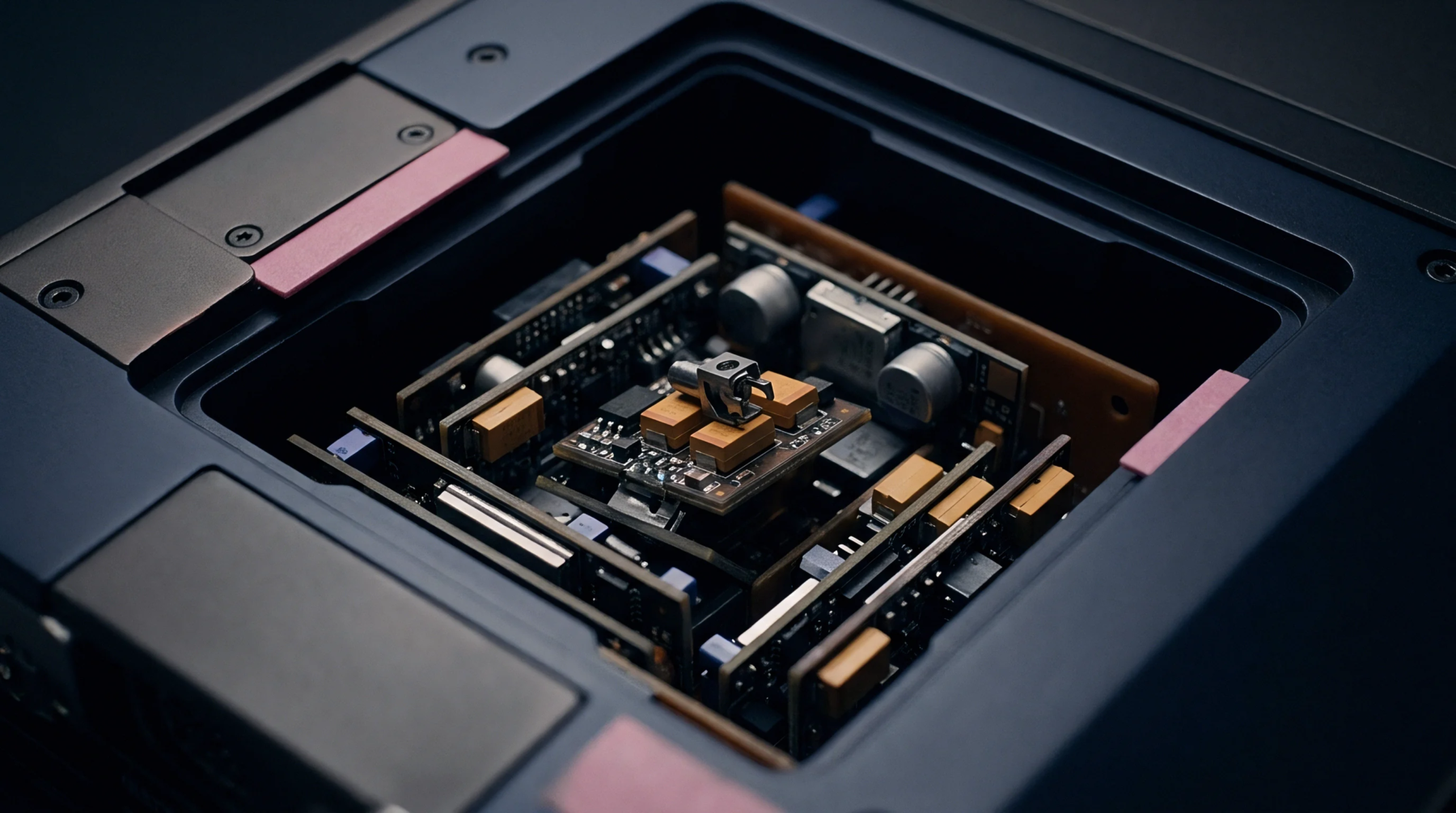
Electronic testing apparatus utilizes an array of spring-loaded pogo pins to establish temporary electrical connections with specific test points located on the surface of a printed circuit board assembly. This mechanical interface allows for the simultaneous measurement of hundreds of signals during the in-circuit testing phase of mass production. By pressing the board against the pins, the bed of nails fixture creates a bridge between the unit under test and the automated test equipment.
This method is faster than using flying probes and provides a repeatable environment for detecting assembly errors. Faults such as short circuits, missing components or incorrect resistor values are identified in seconds. Precision alignment is required to ensure that every pin hits its designated target without damaging the delicate copper pads.
Mechanical Interface
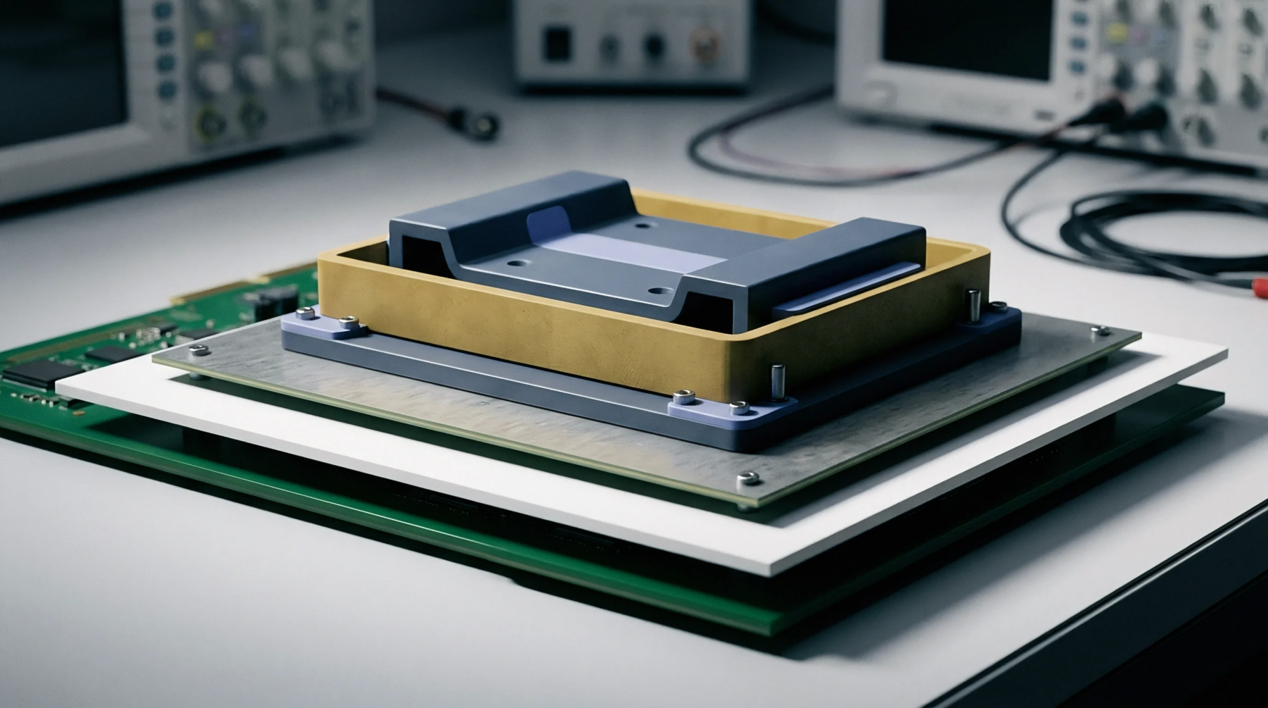
Custom machining of the base plate ensures that the pogo pins are held in the exact coordinates required by the board layout. The bed of nails fixture typically uses a vacuum or pneumatic press to apply even pressure across the entire surface of the assembly. This force must be sufficient to compress the springs and penetrate any residual solder flux on the pads.
If the pressure is uneven, the board might flex, leading to cracked solder joints or broken traces. Designers include specific mounting holes in the board to lock it into position. The selection of pin head shapes, such as pointed, crown or flat, depends on the type of test point being contacted.
Contact Integrity
Reliability of the electrical connection depends on the cleanliness of both the pins and the circuit board. Over time, the bed of nails fixture can accumulate dust and oxidized metal, which increases the contact resistance and leads to false failures. Regular maintenance schedules include cleaning the pins with specialized brushes or ultrasonic baths to maintain conductivity.
High volume production lines often use gold plated pins to resist corrosion and ensure long term performance. If a pin becomes stuck or bent, the test results will become erratic. Engineers monitor the yield rates to identify when a fixture requires refurbishment.
Proper storage of the apparatus in a dry, dust free environment prevents the degradation of the spring mechanisms.
Access Restriction
Layout constraints often limit the number of signals that can be probed on a modern, high density circuit board. Because the bed of nails fixture requires a minimum spacing between pins, engineers must prioritize which nets are essential for testing. Small components and tight trace routing can make it impossible to place a test point on every signal path.
This limitation forces the use of boundary scan or functional testing to supplement the in-circuit measurements. If a critical net is inaccessible, a manufacturing defect might go undetected until the final assembly stage. Designers use specialized software to optimize the placement of test pads during the initial routing phase.
This planning ensures that the test coverage remains high while minimizing the physical footprint of the test points. The final design of the probe map determines the effectiveness of the entire quality control process.