Automated Test Equipment Fixture Escrow Verification and Pogo Pin Degradation Protocols
Verify ATE fixture escrow deposits by executing golden unit loopback tests on independent builds while enforcing pogo pin replacement at 100k cycles.

Fixtures
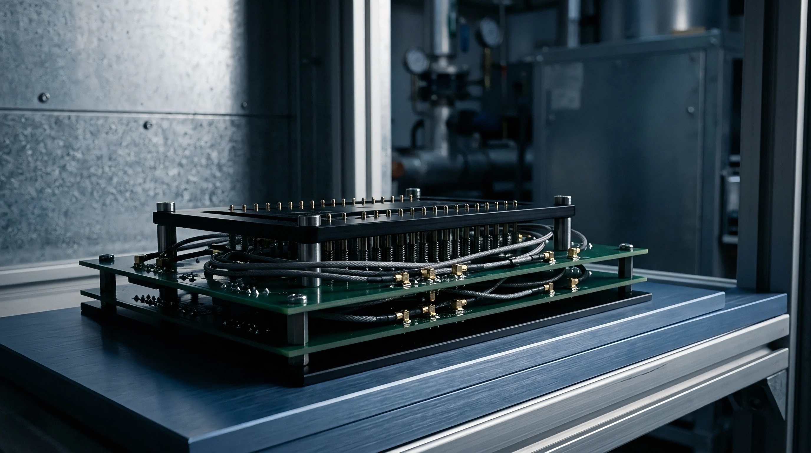
Bed-of-nails automated test equipment relies on physical interface plates that mirror the target printed circuit board assembly. When manufacturing transfers between facilities or contract builders, physical test jigs frequently remain stranded at the original factory. Contractual escrow arrangements resolve this vulnerability by securing complete manufacturing assets offsite, allowing independent reconstitution of the bed-of-nails apparatus.
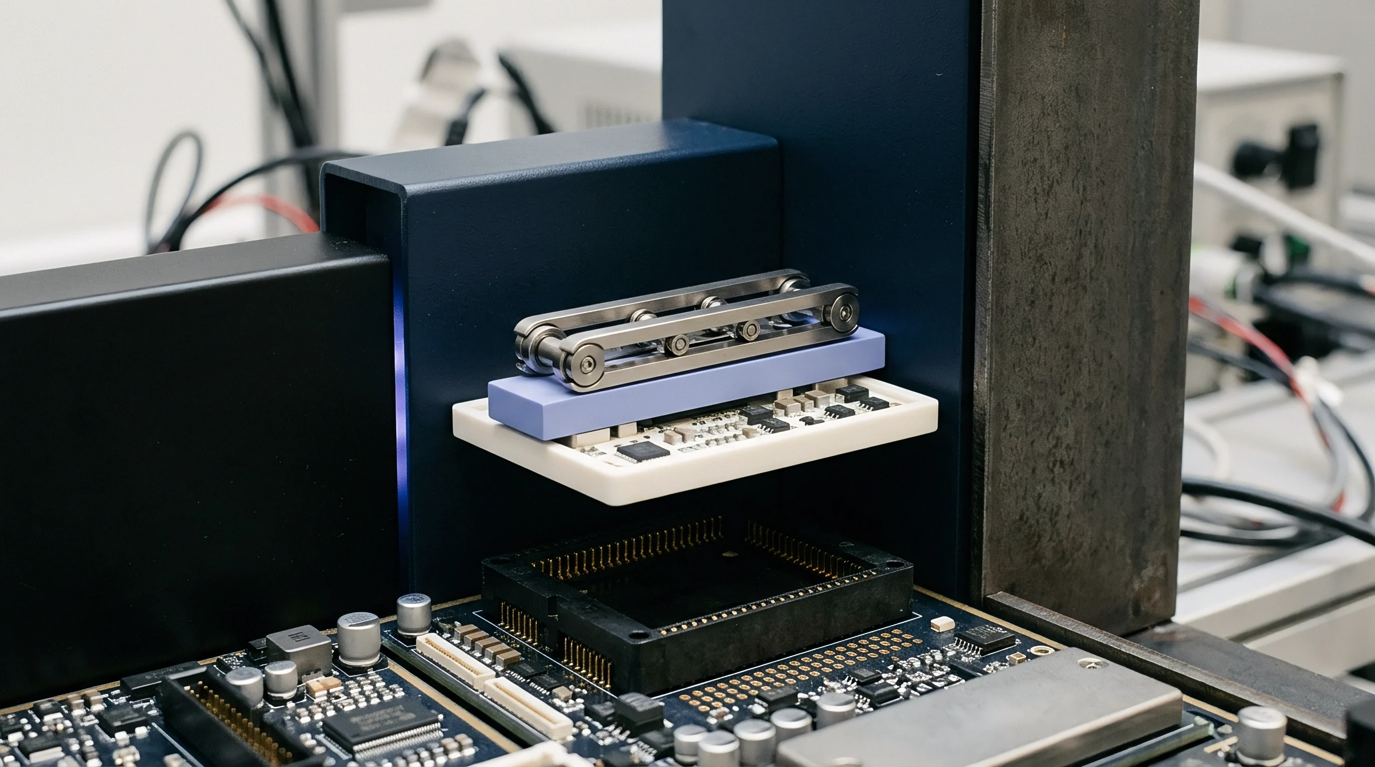
A complete physical deposit package includes the primary raster file, drilling coordinates, top and bottom plate milling specifications, counter-bore depths, spacer block positions, and guide pin offsets.
Deposit Package Architecture
Depositing software code without accompanying physical fixture manufacturing data leaves a test escrow package non-functional. Fixture fabrication requires precise computer-aided design files containing drill location maps, spring probe sizing schedules, wire wrap pin assignments, and cut-out profiles for tall components. Gerber X2 artwork files establish the copper feature boundaries against which the test pin probes align, preventing physical shorts against soldermask edges.
IPC-2581 assembly netlists supply logical node mapping directly to probe receptacle identifiers, allowing test engineers to verify target nodes across routing layers.
Transferring an incomplete deposit halts production during vendor migrations. A functional deposit package contains five distinct design layers that allow an alternate toolmaker to machine replacement plates and wire the probe interface without access to the original factory floor:
- Drill raster files specify hole coordinates, diameter tolerances, and counter-bore depths for probe receptacles within the top plate, push-rod retainers, and bottom guide support structure.
- Wiring harness schematics map pin matrix positions to driver channels on the automated test equipment instrument backplane using explicit net names.
- Mechanical assembly models convey plate separation distance, guide post alignments, latching stroke length, and vacuum sealing gasket profiles in three dimensional step formats.
- Pin receptacle schedules enumerate exact manufacturer part numbers, barrel materials, crimp styles, and wire gauges assigned to every test point coordinate.
- Test sequence source scripts contain uncompiled test vectors, measurement limits, calibration constants, and instrument configuration routines.
Mechanical and Wiring Specifications
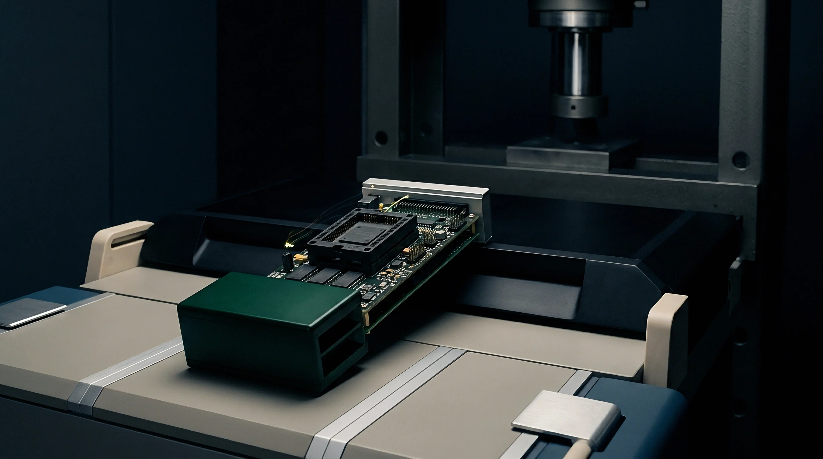
Wiring interface plates by hand introduces parasitic resistance and loop inductance that skew high-frequency analog measurements. Escrow packages define wire gauge, maximum route length, and twisted-pair requirements for every measurement channel. Differential signal paths demand length-matched, shielded coaxial cabling routed directly from the probe barrel tail to the mass interface receiver.
Unshielded point-to-point jumpers over 150 millimeters in length induce crosstalk between adjacent switching nodes, altering pulse timing parameters during high-speed digital functional checks.
A complete fixture deposit package enables an independent machine shop to fabricate a functional bed-of-nails assembly without access to the original vendor.
Vacuum fixtures require separate mechanical CAD definitions for gasketing materials, relief cutouts, and seal compression rates. Moving parts within the fixture suffer wear during push-down cycles, changing the planarity of the board under test relative to the probe field. Escrow documentation details the precise thickness tolerances for polycarbonate top plates and ESD-safe FR4 support structures.
Neglecting plate tolerance specifications causes uneven deflection under vacuum pull, yielding pin bending, cracked solder joints on the target assembly, and premature mechanical fatigue.
Omission of mechanical drawings or netlist files from an escrow deposit forces the buyer to reverse-engineer physical hardware, adding six to ten weeks of downtime during a facility transfer.

Pin
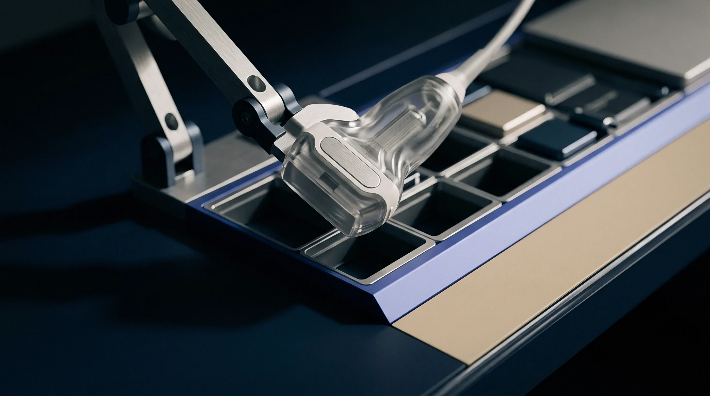
Spring-loaded test probes establish electrical contact with test pads, vias, and component leads on the printed circuit board assembly. These components operate under intense mechanical stress and chemical exposure during volume manufacturing. A standard pogo pin consists of a plunge tip, an internal coil spring, and an outer barrel held within a press-fit receptacle.
Precision contact performance depends entirely on maintaining tight mechanical tolerances and pristine surface metallurgy across millions of micro-actuations.

Contact Surface Metallurgy
Plating materials dictate initial contact resistance and long-term wear resistance. Hard gold over nickel plating remains the industry standard for high-reliability test probes. Gold plating layer thickness typically ranges from 0.75 to 1.25 micrometers, providing low electrical resistance and excellent anti-oxidation characteristics.
Underneath the gold, a nickel sub-layer measuring 1.5 to 3.0 micrometers acts as a diffusion barrier, preventing base metal atoms like copper or beryllium from migrating to the outer surface.
Repeated insertions wear away the outer gold layer, exposing the underlying nickel to ambient air. Exposing nickel causes rapid oxide formation, which increases electrical contact resistance from tens of milliohms to several ohms within a few hundred cycles. Palladium alloy and rhodium contact tips offer superior hardness compared to gold, extending structural lifespan when probing abrasive organic solderability preservative surfaces or oxidized lead-free solder bumps.

Mechanical Fatigue Mechanics
Internal coil springs experience cycle-dependent force relaxation that compromises electrical continuity. Spring wire material selection determines the thermal ceiling and mechanical durability of the probe assembly:
- Beryllium copper springs deliver low electrical resistance and high force stability at operating temperatures up to 120 degrees Celsius.
- Music wire springs provide high force per unit displacement but suffer stress relaxation and susceptibility to corrosion when operating above 85 degrees Celsius.
- Stainless steel springs resist elevated temperatures up to 200 degrees Celsius and withstand corrosive flux residues, though they exhibit higher internal electrical resistance.
- Specialty spring alloys maintain structural force elasticity across high temperature burn-in cycles exceeding 250 degrees Celsius.
Plunger tip geometry directly influences contact reliability through flux residue and surface contaminants. Spear-point and chisel tips penetrate surface oxides and non-conductive rosin residue, concentrating mechanical force onto a minimal surface area. Flat, spherical, and multi-faceted cup tips reduce pad cratering and board surface marks but require clean, unoxidized test pads to maintain low contact resistance.
Debris accumulation inside the plunger cup causes tip tilt, resulting in binding within the barrel sleeve.
Probes operating past their mechanical actuation rating display spring force attenuation, causing erratic functional failures that appear to originate from component batch defects rather than unmaintained fixture tooling.
Decay
Degradation of test probes follows predictable non-linear curves governed by insertion cycles, current density, and environmental contamination. Contact resistance remains stable during the initial phase of operation, where surface plating remains intact. Once micro-abrasion strips the primary gold layer, contact resistance drifts upward unpredictably.
Unmonitored resistance degradation introduces false failures into production lines, triggering unneeded re-work cycles and corrupting line yield statistics.

Contact Resistance Attenuation
High electrical current passing through small contact surface areas generates localized Joule heating. Micro-welding occurs when localized temperatures exceed the melting threshold of the tip plating material, creating surface roughness, metal transfer, and cratering. Current surges exceeding probe ratings cause rapid annealing of the internal coil spring, destroying spring temper and reducing downward mechanical force.
| Plating Material | Hardness (Knoop) | Initial Contact Resistance (mΩ) | Rated Insertion Cycles | Primary Failure Mode |
|---|---|---|---|---|
| Gold over Nickel | 130 – 200 | < 20 | 100,000 | Gold wear-through and nickel oxidation |
| Palladium Alloy | 350 – 450 | < 35 | 300,000 | Debris accumulation in tip contours |
| Rhodium | 600 – 800 | < 50 | 500,000 | Micro-cracking from thermal stress |
| Electroless Nickel | 400 – 500 | < 80 | 50,000 | Rapid surface passivation |
| Data based on continuous testing at 2.0 Amps continuous current and 50 grams contact force in dry ambient conditions. | ||||
Sub-milliohm voltage drop shifts distort high-precision analog measurements. For example, testing low-dropout voltage regulators or current-sense amplifiers requires millivolt accuracy. When pogo pin degradation adds 500 milliohms of parasitic resistance to a ground probe line, the functional tester records an artificial voltage offset, rejecting functional boards.
Unmanaged degradation converts test fixtures from quality verification instruments into sources of systematic yield loss.
Yield Measurement Errors
Contamination accumulation accelerates probe degradation. Solder flux particles, organic outgassing residues, and ambient dust gather on the plunger tip, forming an insulating barrier. Solder flux deposits harden under repeated thermal cycles, increasing contact resistance exponentially over brief production windows.
A contact resistance increase of 200 milliohm on a power rail pin induces false voltage drop failures during functional board testing.
Calculating overall test yield decay requires tracking both open-circuit false failures and intermittent high-resistance contacts. False fail rates scale directly with total actuation count, creating a clear wear profile. Plotting false fail frequency against cycle count establishes the precise window where preventive maintenance must intervene before yield loss costs surpass probe replacement costs.
Distinguishing true printed circuit board component defects from pogo pin degradation requires active tracking of probe metrics during high-volume production runs.
Receipt
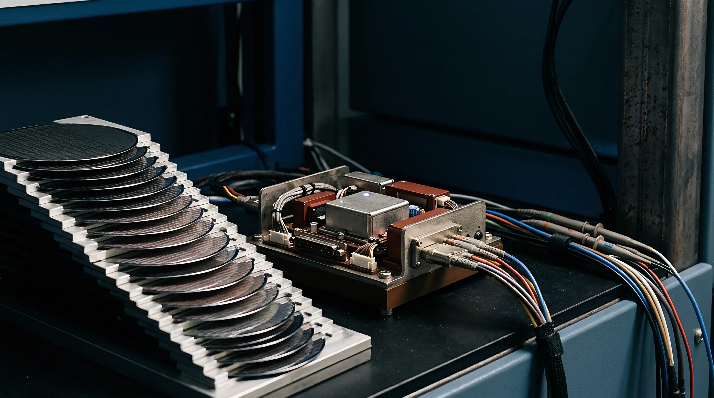
Escrow verification ensures that physical fixture assets held in storage match the operational environment active on the manufacturing floor. When escrow packages are released following contract termination or vendor insolvency, the buyer must validate that the deposited files can reproduce working test fixtures. Verification requires extracting the deposit files, building a prototype fixture or auditing an existing unit, and validating performance against known golden units.
Golden Unit Loopback Procedures
Golden units serve as calibration standards for validating escrowed test fixture designs. A golden unit comprises a fully verified printed circuit board assembly with known electrical parameters and tight component tolerances. Installing a golden unit into a newly fabricated escrow fixture verifies mechanical alignment, pin target contact accuracy, and signal integrity across all measurement nodes simultaneously.
- Load escrowed software scripts into an isolated automated test bench environment without active network connections.
- Extract CAD drill files and wire netlists from the escrow archive and verify digital signature checksums against escrow records.
- Fabricate a physical test plate using the extracted drill files and populate it with new, calibrated pogo pin receptacles.
- Wire the test plate according to the escrowed wiring netlist using specified wire gauges and signal routing limits.
- Install the assembled fixture onto the target automated test station and execute system diagnostic self-tests.
- Insert the reference golden board and execute the full test suite twenty consecutive times to establish baseline measurement distributions.
- Compare measurement outputs against archived reference logs to verify node-level statistical parity.
Can Escrow Deposit Hashes Prevent Substitution?
Cryptographic hash verification guarantees file integrity but fails to detect functional mismatches caused by unrecorded physical fixture modifications. Wire routing adjustments, added bypass capacitors, or pin tip changes made on the factory floor to optimize yield often go unrecorded in the central CAD repository. These undocumented field changes leave the escrowed files out of sync with active factory tooling.
Executing an escrow audit requires cross-referencing file hashes while simultaneously validating physical wire topologies against compiled test scripts.
Audit protocols require periodic physical inspections comparing active factory fixtures directly against escrowed records. Measuring wire lengths, verifying pin part numbers, and sampling spring force across the bed of nails catches unrecorded modifications before emergency deposit releases occur. Discrepancies between active fixtures and escrow deposits must trigger immediate update cycles funded by the party responsible for fixture maintenance.
Verification routines that skip golden unit functional validation risk accepting incomplete fixture deposits that fail during emergency assembly bring-up.


Contract
Escrow agreements for automated test equipment depend on clear definitions of ownership, access rights, and maintenance obligations. Fixture engineering scope spans multiple service tiers, from turnkey solutions where the factory owns the fixture assets to semi-custom arrangements where intellectual property transfers to the buyer upon final non-recurring engineering payment. Clarifying asset boundaries prevents expensive legal disputes when shifting production between contract electronics manufacturers.

Maintenance Allocation and SLA Pricing
Turnkey contracts bundle fixture fabrication, pin replacement, and yield performance guarantees into a single unit price or NRE fee. Semi-custom models separate physical asset ownership from operational maintenance, leaving the buyer responsible for probe wear costs and fixture re-calibration. Defining explicit Service Level Agreements for pogo pin maintenance establishes clear operational boundaries.
| Integration Scope | Fixture NRE Ownership | Pogo Pin Maintenance Responsibility | Escrow File Access Rights | Transfer Lead Time |
|---|---|---|---|---|
| Turnkey Integrated | Factory retained | Factory funded and executed | Restricted to compiled binaries | 12 to 16 Weeks |
| Semi-Custom Sourced | Buyer owned upon final payment | Shared based on cycle limits | Full source files and CAD drawings | 2 to 4 Weeks |
| White-Label Reference | Shared joint ownership | Buyer funded, factory executed | Source files released under escrow trigger | 6 to 8 Weeks |
SLA clauses must define maximum allowable contact resistance thresholds, mandatory pin replacement cycle intervals, and false failure rate caps. A standard clause mandates pogo pin field replacement every 100,000 insertions or whenever channel contact resistance exceeds 100 milliohms during continuous operation. Amortizing replacement probe costs into the unit price aligns factory incentives toward maintaining low false failure rates and pristine test interfaces.
Escrow Release Triggers
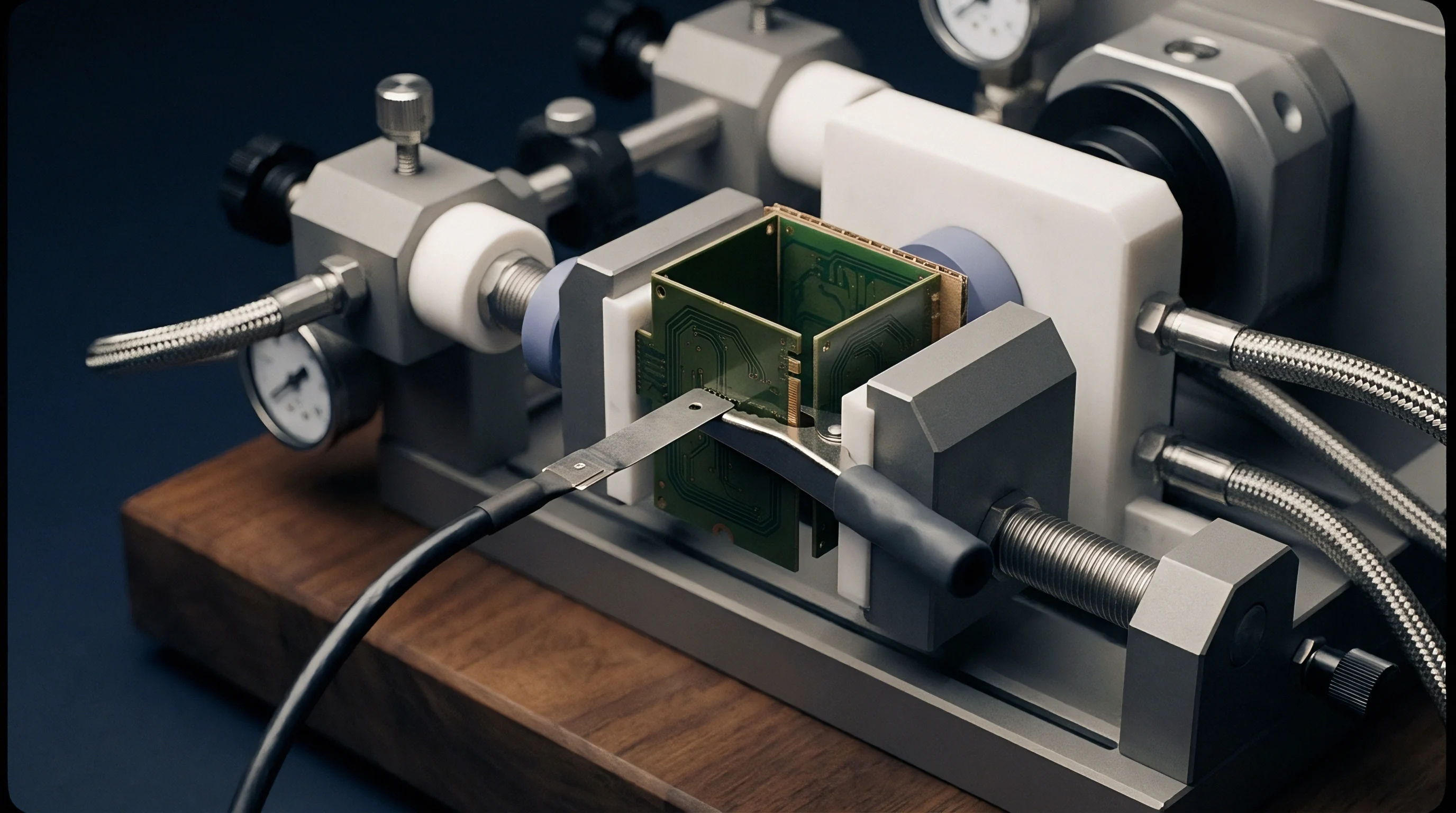
Escrow release clauses outline explicit conditions under which physical CAD data, wiring netlists, and test script source code move to the buyer. Standard triggers include contract termination, vendor insolvency, failure to meet agreed production capacity, or persistent yield degradation stemming from poor fixture maintenance. Escrow agents require verifiable technical verification before executing releases, preventing improper intellectual property transfers during routine commercial disputes.
- Insolvency trigger lines mandate immediate release of physical fixture assets and CAD repositories upon formal bankruptcy filings.
- SLA breach provisions grant escrow access if the manufacturing facility fails to rectify systemic yield loss within fourteen days of written notice.
- Capacity failure clauses enable escrow release when the factory cannot meet scheduled order volumes due to test equipment downtime.
- Commercial transition covenants establish smooth asset handovers upon contract expiration, requiring active factory support during dual-sourcing setup.
Per section 14.2 of standard electronics manufacturing service agreements, all fixture design files, pogo pin map schematics, and uncompiled test scripts shall automatically transfer to the buyer upon settlement of all outstanding non-recurring engineering invoices.