Calculating Unit Cost Break-Even Points for Semicustom Wireless Modules
Semicustom wireless module break-even hinges on offsetting upfront NRE and regulatory fees against unit BOM savings across yield-adjusted volume thresholds.


Silicon
Choosing where to set the integration boundary for a wireless subsystem directly affects unit hardware cost, board real estate, and upfront NRE charges. Standard off-the-shelf modules enclose the transceiver IC, crystal oscillators, power management passives, and RF front-end circuitry on a dedicated substrate beneath a metal shield. While this setup bypasses antenna matching iterations and basic regulatory testing on the host board, that convenience adds a permanent BOM penalty of 1.80 USD to 4.20 USD per unit over discrete components.
Semicustom wireless modules shift this tradeoff by adopting existing silicon reference designs while altering the substrate footprint, pinouts, or integrated passive networks. When a design requires tight mechanical tolerances, high-density interconnections, or integrated bandpass filters, standard modules often force the use of auxiliary carrier boards that raise assembly labor. Moving custom impedance matching and low-noise amplifiers directly onto a modified module substrate clears those external surface-mount components off the main motherboard.

Architecture Selections across Integration Depths
Moving from early prototypes to mid-scale production usually means choosing between three levels of integration. Standard surface-mount modules give you pre-certified radio functionality at the cost of rigid routing options and pad layouts. Fully discrete designs place the transceiver IC and every passive component straight onto the main application board ~ maximizing spatial efficiency, but putting all RF layout responsibility on the design team.
Semicustom modules sit between these extremes, putting validated RF layouts onto a tailored substrate.
Component choices inside a semicustom module affect both initial mask tooling and ongoing placement costs. Using standard surface-mount passives (0201 or 0402 packages) under the module shield keeps substrate fabrication costs down. Embedded passives ~ etching capacitors and inductors straight into the inner laminate layers ~ clear off top-layer space, though at the cost of higher laminate tooling fees.
| Integration Level | Upfront NRE Range (USD) | Average Unit BOM Shift | Host PCB Area Impact | Certification Scope |
|---|---|---|---|---|
| Standard Off-the-Shelf Module | 0 – 5,000 | Baseline (+0.00 USD) | High (150 mm² to 300 mm²) | Pre-certified (Modular Grant) |
| Semicustom Substrate Module | 25,000 – 75,000 | -1.20 to -2.80 USD | Medium (80 mm² to 140 mm²) | Class II Permissive Change |
| Full Discrete Board Design | 80,000 – 180,000 | -2.50 to -4.50 USD | Low (40 mm² to 90 mm²) | Full Intentional Radiator (FCC/CE) |

Front End Integration and Passive Reduction
RF performance hinges on impedance matching between the power amplifier, antenna switch, and antenna structure. Evaluation boards show clean 50-ohm matching on neat four-layer FR4 substrates with controlled dielectric constants, but moving that exact layout onto a custom host PCB ~ with a different stackup, nearby plastics, or an adjacent battery ~ pulls the resonant frequency off target.
Semicustom modules avoid stackup sensitivity by pulling the matching network, low-noise amplifier, and harmonic filters onto an independent, tightly controlled substrate layer. Keeping the dielectric environment stable around the front end holds high-frequency losses predictable across motherboard manufacturing lots. Dropping discrete filter components off the main board also cuts pick-and-place cycles, lowering defect rates during assembly.
At fifty thousand units annually, shifting four passive impedance circuits into a custom substrate reduces surface-mount placement operations by twelve thousand per batch.
One lingering uncertainty is whether silicon foundries will guarantee supply of current transceiver die variants without forcing package migrations across a five-year production cycle.

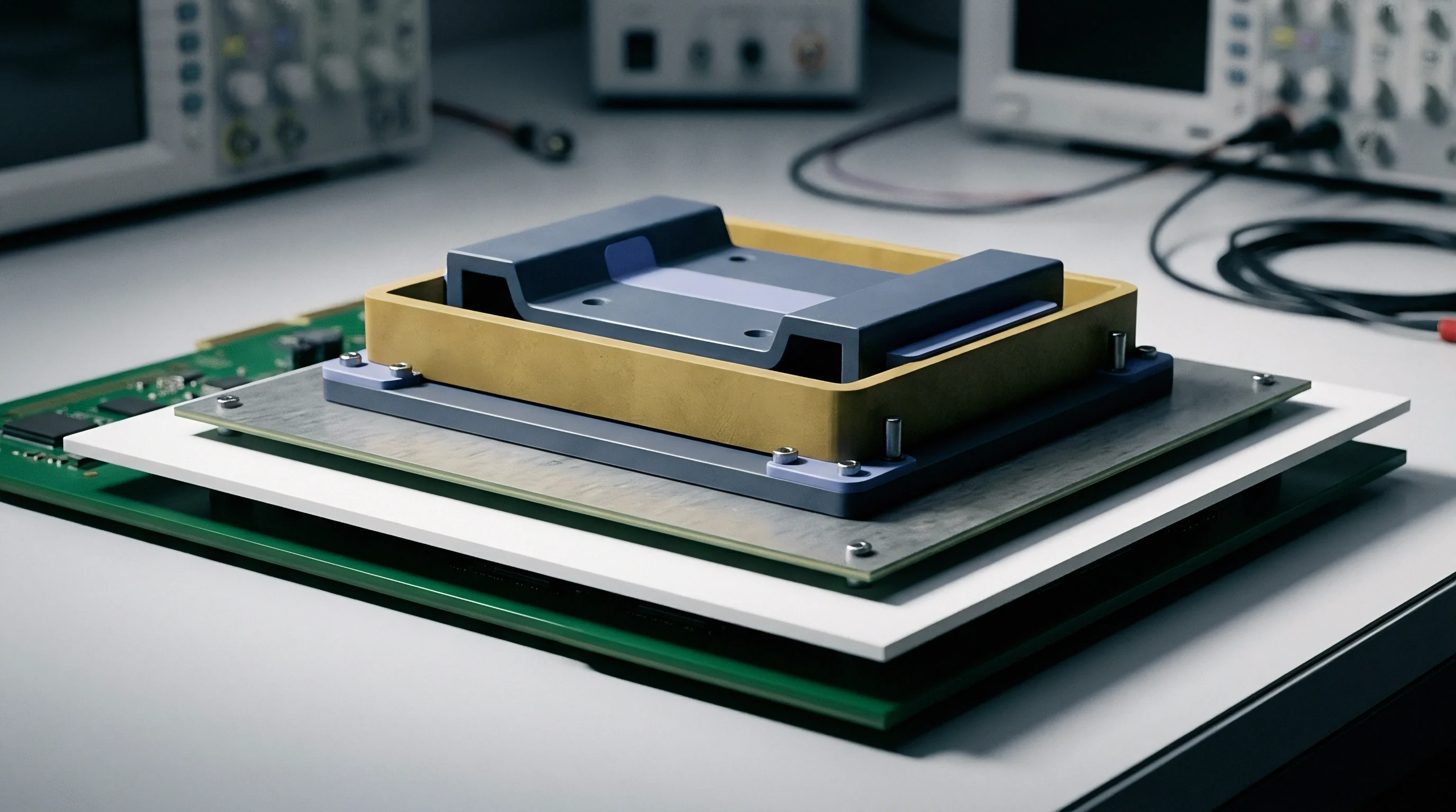
Work
Upfront NRE represents the main barrier when stepping up from standard modules to semicustom builds. Scope creep during development quickly eats into projected financial returns. Engineering work generally breaks down into five distinct tasks: substrate layout, antenna tuning, firmware driver porting, environmental stress testing, and regulatory pre-compliance screening.

Non-Recurring Engineering Scope Elements
Substrate design takes specialized RF layout experience to keep noisy digital buses away from sensitive analog front ends. Layout engineers spend considerable time tuning ground plane continuity, microstrip trace widths, and via fencing. Fabrication houses then charge custom substrate tooling fees to cover photolithography masks, drill program validation, and electrical test fixtures.
Antenna matching and enclosure tuning take up another large portion of the engineering budget. Enclosing a wireless module in plastic or metal changes its impedance, requiring electromagnetic simulations, vector network analyzer measurements, and passive value iterations to hit total radiated power and total isotropic sensitivity targets.
| Engineering Work Package | Primary Skill Domain | Typical Hours | Deliverable Artifact |
|---|---|---|---|
| Substrate Layout & Stackup Design | RF Printed Circuit Board CAD | 60 – 120 | Gerber X2 / ODB++ Package |
| Antenna Matching & Co-design | Electromagnetic Simulation | 40 – 90 | S-Parameter Test Dossier |
| Board Support Package Adaptation | Embedded C / RTOS Drivers | 80 – 160 | Validated Firmware Repository |
| Pre-Compliance RF Screening | Compliance Engineering | 30 – 60 | Anechoic Chamber Test Report |

Verification Jigs and Software Stack Calibration
System bring-up relies heavily on custom hardware verification jigs and test scripts. Because semicustom modules often feature unique pad layouts, factory end-of-line testing usually requires custom bed-of-nails fixtures. Hardware engineers develop these fixtures alongside the main module so automated test equipment can verify RF output power, frequency offset, and current draw on the line.
- Audit the supplier engineering scope document to verify that Gerber X2 file outputs, schematics, and bill-of-materials databases belong entirely to the buyer upon final payment.
- Establish fixed performance criteria for receiver sensitivity and harmonic suppression before authorizing substrate tooling expenditures.
- Require the engineering provider to deliver complete build scripts and source code for factory test firmware tools rather than compiled binary files.
- Validate regulatory status by determining whether modified layout structures qualify for a Class II Permissive Change or demand full intentional radiator certification.
Software stack adjustments are another common labor sink. Off-the-shelf modules typically ship with vendor firmware that handles network association, security handshakes, and low-power sleep states out of the box. Switching to a semicustom design often forces engineering teams to port hardware abstraction layers, adjust pin mappings, and re-verify power draw across every sleep state.
A low initial non-recurring engineering quotation frequently shifts unstated development hours onto the buyer during post-qualification bring-up.
Cutting corners on pre-compliance chamber testing frequently leads to failed formal regulatory audits, which doubles certification costs and delays volume shipments.

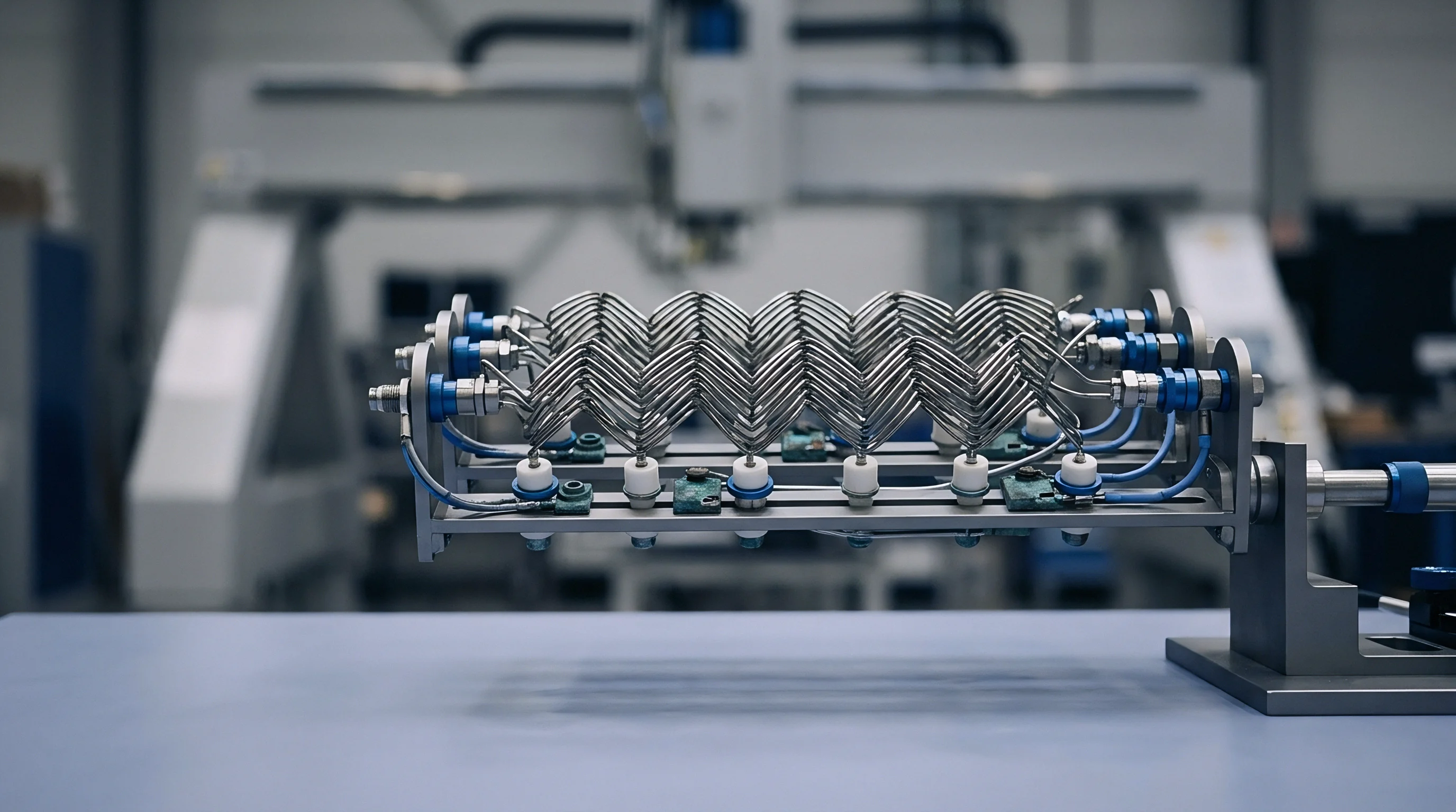
Yield
Unit pricing at the assembly plant depends heavily on yield, component tolerances, and screening overhead. A lower quoted BOM cost offers no real savings if scrap rates jump at the assembly house. High-frequency wireless modules are sensitive enough that small variations in solder volume or placement shift key radio performance metrics.

How Does Test Coverage Expansion Alter Unit Margins?
Factory test coverage directly drives unit transformation costs. Basic continuity and power-rail checks confirm electrical assembly, but they miss subtle RF defects. Full RF end-of-line testing measures transmitter error vector magnitude, carrier frequency drift, and receiver bit error rates across several channels.
Deeper test coverage extends cycle times on expensive vector signal analyzers. Running a forty-five second test sequence on every module adds significant overhead compared to a ten-second basic screening routine, forcing teams to balance higher factory test costs against the risk of shipping defective radios to customers.

Factory Screening and Defect Density Shifts
Defect rates rise quickly when component placement tolerances or thermal reflow profiles drift. Semicustom modules using fine-pitch ball grid arrays carry higher risks of solder bridging than standard leaded packages.
- Solder Voiding Under Ground Pads leads to elevated thermal resistance and degraded RF ground return paths, causing intermittent transmitter distortion during high-power bursts.
- Crystal Oscillator Frequency Offsets caused by mechanical stress or improper loading capacitance prevent network synchronization on narrow-band channels.
- Passive Component Value Drift during reflow soldering shifts impedance matching networks, degrading receiver sensitivity metrics by several decibels.
- Shield Can Deformation during automated placement creates internal electrical shorts against tall surface-mount components inside the module enclosure.
An assembly line running at ninety-two percent first-pass yield passes the cost of scrapped substrates and rework directly into the finished unit price. Clear yield agreements set baseline thresholds, requiring the plant to absorb component losses whenever first-pass yield drops below contract numbers.
Weak screening at the substrate level risks latent field failures, leading to costly warranty recalls and reputational damage.

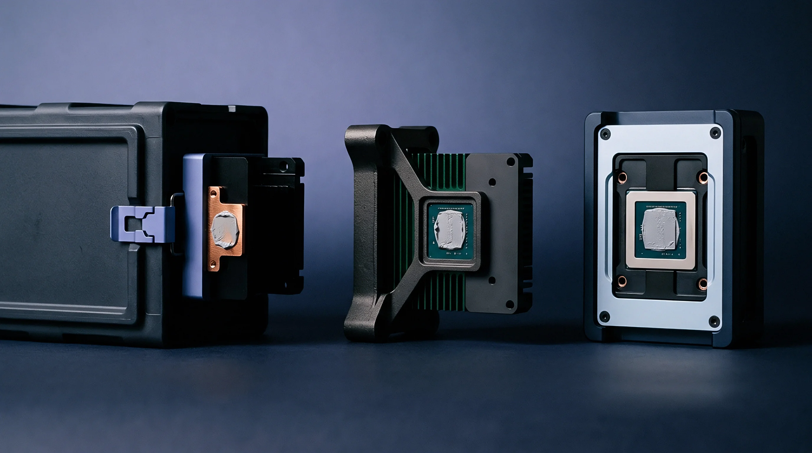
Ledger
Finding the true break-even volume between off-the-shelf modules and semicustom designs requires a full financial model. That calculation has to combine upfront NRE, substrate tooling, regulatory certification, per-unit hardware savings, and factory test overhead. A simple payback estimate that ignores recertification or ongoing software maintenance gives an unrealistically optimistic timeline.

Mathematical Break-Even Modeling
The break-even formula identifies the exact volume where total spending on a semicustom build matches the ongoing cost of off-the-shelf modules. While standard module costs scale linearly with volume, semicustom economics start with a steep fixed NRE step followed by a shallower per-unit cost curve.
Let initial non-recurring engineering, substrate tooling, test jig development, and regulatory certification costs total fixed capital expense (F). Let the unit purchase price of the standard module equal baseline unit cost (C_std). Let the unit production cost of the semicustom module equal custom unit cost (C_cust), incorporating raw components, substrate manufacturing, factory assembly, and test time.
The basic break-even volume (V_be) evaluates as:
V_be = F / (C_std – C_cust)
Real-world financial models must expand this baseline formula to account for volume-based tiered pricing, yield penalty factors (Y), and annual ongoing software maintenance fees (M). The complete total cost equation over a multi-year horizon equates total standard spending against custom expenditure:
V C_std(V) = F + (V (C_cust(V) / Y)) + (T M)
Where T represents production duration in years, C_std(V) and C_cust(V) represent volume-dependent unit price functions, and Y represents the fractional first-pass yield rate (for example, 0.95 for 95% yield).
| Total Upfront Investment (F) | Unit Cost Delta (C_std – C_cust) | Calculated Break-Even Volume | Yield Adjusted Break-Even (95% Yield) | Three-Year Break-Even with Maintenance |
|---|---|---|---|---|
| 40,000 USD | 1.50 USD | 26,667 units | 28,421 units | 32,421 units |
| 60,000 USD | 2.20 USD | 27,273 units | 28,986 units | 31,713 units |
| 90,000 USD | 2.80 USD | 32,143 units | 34,068 units | 36,211 units |
| 130,000 USD | 3.40 USD | 38,235 units | 40,568 units | 42,627 units |

Worked Scenario across Multi-Tier Volume Vectors
Consider a concrete example. An industrial sensor manufacturer currently buys a pre-certified Bluetooth Low Energy off-the-shelf module at 5.50 USD per unit for an annual volume of 20,000 units. A module integrator proposes a semicustom alternative.
The custom design costs 2.70 USD per unit in component BOM and assembly fees. Upfront expenditures include 35,000 USD for RF layout and antenna matching NRE, 12,000 USD for automated test jigs, and 18,000 USD for FCC/CE Class II Permissive Change filings and lab testing ~ bringing total upfront investment (F) to 65,000 USD.
- Unadjusted Unit Margin Delta yields a net unit savings of 2.80 USD (5.50 USD minus 2.70 USD). The simple break-even volume calculates to 23,215 units, achievable in roughly fourteen months at baseline production rates.
- Yield-Adjusted Production Accounting incorporates a realistic 96 percent assembly yield rate. Effective unit price becomes 2.81 USD (2.70 USD divided by 0.96), reducing unit savings to 2.69 USD. The yield-adjusted break-even shifts outward to 24,164 units.
- Lifecycle Maintenance Integration adds 6,000 USD per year in firmware stack security updates and component lifecycle tracking. Over a three-year window, total fixed and maintenance costs reach 83,000 USD, pushing the operational break-even point to 30,855 units.
Under IPC-A-610 Class 2 standards, functional testing failures at final assembly forfeit component recovery rights unless vendor defect responsibility is explicit.
Initial non-recurring engineering fees are sometimes presented as covering long-term substrate tooling maintenance, only for additional re-tooling charges to appear when volume runs extend into secondary production batches.

Transfer
Design ownership and manufacturing rights dictate whether a buyer maintains supply chain flexibility or gets locked into a single vendor. A semicustom module developed under a vague engineering services agreement often leaves core intellectual property in the hands of the design house. Moving production to a second-source facility requires full access to design source files, manufacturing documentation, and firmware build environments.
Ownership Rights and Escrow Architecture
Contracts need to distinguish clearly between background IP brought into the project by the module vendor and foreground IP generated during development. Background IP typically covers generic radio drivers, proprietary hardware abstraction layers, and reference layouts. Foreground IP includes the specific schematic topologies, custom substrate stackups, board physical dimensions, and application-specific pinouts.
- Native CAD Design Databases containing complete Altium, Cadence Allegro, or KiCAD schematic and layout source files rather than flat PDF drawings.
- Manufacturing Output Packages incorporating Gerber X2 or IPC-2581 files, NC drill files, pick-and-place coordinate files, and assembly drawings.
- Firmware Source Repositories containing raw C/C++ source code, build scripts, linker scripts, toolchain definitions, and underlying SDK dependencies.
- Test Jig Construction Specifications including schematic diagrams, mechanical pin-bed drawings, and executable test software source code.
IP escrow provides an important safety net when working with proprietary module designs. Placing source code and fabrication files in an independent escrow vault guarantees release if the primary module supplier enters insolvency, defaults on delivery commitments, or sunsets the product line.

Second Source Qualification Expenditure
Qualifying a second source for a semicustom module requires upfront capital that impacts long-term break-even calculations. Bringing on a secondary supplier involves fabricating trial substrate lots, assembling verification samples, and running comparative RF performance audits.
Qualifying a second manufacturing source generally costs between 15,000 USD and 35,000 USD in engineering time and trial runs. While this investment pushes out the overall break-even threshold, it protects volume production against factory downtime, tariff shifts, or component shortages.
The manufacturing agreement should specify that once agreed NRE milestones are paid, the buyer holds an irrevocable, worldwide, royalty-free license to manufacture, modify, and sub-license the module hardware layout and board support package firmware across secondary production facilities.