Meaning
A native or thermally grown thin insulating film forms between a metallic layer and an underlying semiconductor or conductive substrate. An unwanted or intentionally grown interfacial oxide layer alters electrical conduction across metal contacts and gate dielectric stacks. The impact of this oxide layer diminishes when film thickness falls below atomic monolayer dimensions or when chemical etching fully removes native films prior to metallization.
Growth Mechanism
Exposure of bare silicon or metallic surfaces to atmospheric oxygen forms a self-limiting native oxide within minutes. Uncontrolled growth of interfacial oxide creates non-uniform film thickness across contact surfaces, causing contact resistance variation across circuit boards.
Electrical Conduction
Thin native oxides act as potential barriers that force electric current to flow through quantum tunneling rather than ohmic conduction. Presence of an interfacial oxide increases contact resistance and introduces non-linear current-voltage behavior in high-frequency signal paths. In spring-loaded connector contacts, high normal forces are required to physically disrupt oxide films and restore low-resistance metallic contact, preventing signal degradation in multi-band radio assemblies.
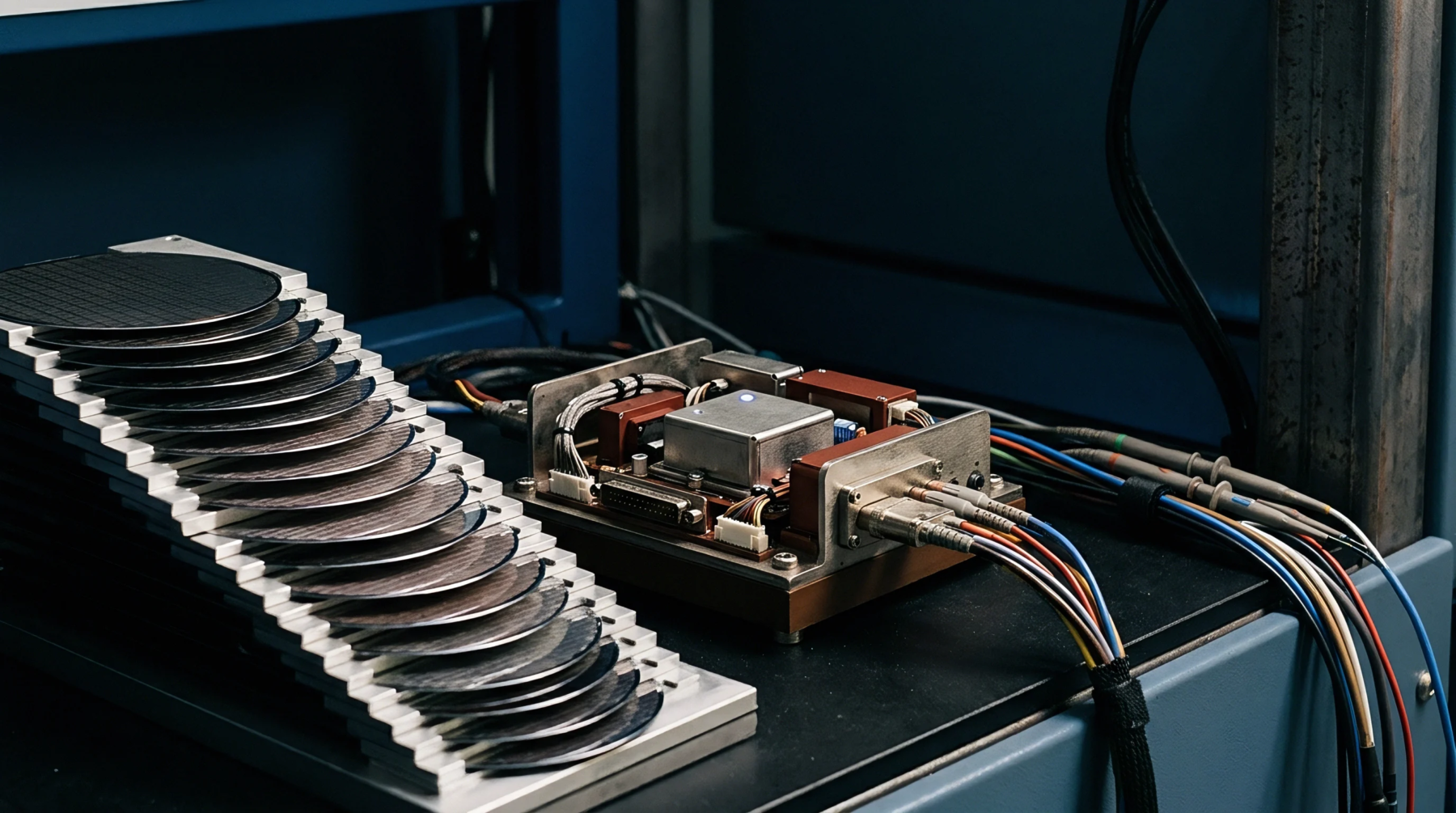
Network analyzers measure signal attenuation caused by oxide-induced contact resistance.
Process Control
Surface preparation protocols utilize hydrofluoric acid dips or plasma cleaning steps to strip native oxide layers immediately prior to metal deposition. Controlled annealing steps react residual interfacial oxide with active gate metals to form stable silicate layers. Process traveler records confirm pre-metallization etch duration and vacuum queue times.