Evaluating Radio Frequency Signal Attenuation Shifts Induced by Contact Oxide Accumulation
Contact oxide growth adds up to 3 dB insertion loss in RF interconnects, degrading link margin and driving retransmissions unless wiping force exceeds 0.3 N.

Junction
Mechanical interconnections using pressure spring fingers, pogo pins, or coaxial board-to-board connectors undergo microscopic surface changes when exposed to ambient air. Base substrate metals like copper, beryllium-copper, and brass react naturally with oxygen, sulfur, and atmospheric moisture. Even beneath thin decorative flash coatings, base metal atoms diffuse outward along grain boundaries to form passivation films composed of semi-conductive oxides such as cuprous oxide, cupric oxide, and nickel oxide.
These surface oxide layers directly impair high-frequency signal propagation across the interface.
At low direct current, an intact oxide dielectric layer forms a physical barrier to electron transport. Direct conduction occurs primarily through microscopic high points where mechanical force physically shears the oxide film to form true metal-to-metal conducting spots, known as a-spots. Surrounding these localized metallic bridges, thin oxide regions measuring between 1 nanometer and 20 nanometers thick allow quantum mechanical electron tunneling.
As environmental thermal cycling and humidity accelerate chemical growth, the total metallic conducting area shrinks, raising resting contact resistance and introducing non-linear current-voltage behavior at the interface.
Gold flash coatings thinner than 0.1 micrometers permit substrate nickel migration to the outer interface within six months under 85 degrees Celsius and 85 percent relative humidity testing.
Microscopic oxide accumulation introduces specific electrical breakdown phenomena when subjected to changing excitation levels. High voltage potential can induce dielectric breakdown across ultra-thin film regions, a physical mechanism known as fritting. A-spot breakdown drops interface resistance instantaneously by melting conductive channels through the oxide layer.
Small RF signals operating below the dielectric breakdown potential lack the voltage swing to initiate fritting, causing the non-linear oxide dielectric to remain fully intact across the contact area.
Interconnect performance degrades through distinct chemical and mechanical pathways during prolonged field operation:
- Base Metal Substrate Migration occurs when copper or nickel atoms diffuse through porous thin-gold surface layers, forming dense non-conductive oxide films directly on the outer contact face.
- Fretting Corrosion Degradation develops under micro-motion caused by structural thermal expansion or vibration, continually breaking pristine metallic contact spots and exposing fresh metal to immediate oxidation.
- Sulfidation and Chloridation Contamination forms thick tarnishing layers when atmospheric sulfur dioxide or airborne marine salt ions react with exposed copper or silver spring fingers.
- Moisture Capillary Condensation draws ambient water vapor into microscopic surface asperities, accelerating galvanic oxidation between dissimilar metal underplates.
Elevated high-frequency insertion loss is frequently attributed to mechanical board misalignment, though sub-micrometer gold flash coatings actually permit base substrate nickel to migrate to the outer contact face within months of field deployment.

Impedance
Alternating current at microwave frequencies exhibits non-uniform current distribution across conductive cross-sections due to electromagnetic self-inductance. As operating frequency increases, electromagnetic fields force signal currents into a thin outer region near the conductor perimeter. The operational thickness of this conductive channel, designated as the electromagnetic skin depth, decreases inversely with the square root of frequency and magnetic permeability.

Frequency Dependent Skin Depth and Surface Losses
High-frequency current flows almost entirely within the outermost micrometers of a contact structure. At 900 MHz, the electromagnetic skin depth in pure copper measures approximately 2.18 micrometers. Elevating the signal frequency to 2.4 GHz reduces this depth to 1.33 micrometers, while at 5.8 GHz the current concentrates within a shallow layer measuring 0.86 micrometers thick.
When base metal oxidation establishes a semi-insulating film across the outer interface, high-frequency current encounters a high-resistivity boundary layer directly within its primary conduction path, where dense oxides disrupt direct metallic continuity.
Instead of traversing a uniform metallic conductor, high-frequency current must cross narrow metallic a-spots or bridge thin dielectric oxide gaps via parasitic capacitance. The effective electrical model transforms from a simple low-value resistance into a complex parallel network of contact resistance, non-linear tunneling resistance, and boundary capacitance. This parasitic capacitive component introduces frequency-dependent signal phase shifts and amplitude attenuation, severely degrading signal transmission metrics across wide bandwidths.
As a result, signal current crowds into tiny remaining contact spots.
| Frequency Band | Oxide Film Thickness (nm) | Normal Contact Force (N) | Insertion Loss Shift S21 (dB) | Return Loss Shift S11 (dB) |
|---|---|---|---|---|
| 868 / 915 MHz | 5.0 | 0.50 | 0.12 | -0.8 |
| 868 / 915 MHz | 25.0 | 0.15 | 0.85 | -3.2 |
| 2.4 GHz | 5.0 | 0.50 | 0.35 | -1.5 |
| 2.4 GHz | 25.0 | 0.15 | 1.90 | -6.4 |
| 5.8 GHz | 5.0 | 0.50 | 0.80 | -3.1 |
| 5.8 GHz | 25.0 | 0.15 | 3.45 | -11.8 |

When Does Contact Fritting Break Small-Signal RF Links?
Transmitters broadcasting high RF power levels generate peak-to-peak voltage swings across demountable interfaces capable of exceeding the dielectric breakdown threshold of thin oxide layers. When local electric field intensity exceeds several megavolts per centimeter, micro-dispersion electrical fritting punches conductive filamentary channels through the insulating film, restoring low-resistance metallic contact. Low signal levels, however, leave these dielectric oxide barriers intact.
Receivers working near sensitivity limits operate with voltage amplitudes below one millivolt RMS across a 50-ohm load. These low amplitudes remain far below the 20 to 100 millivolt potential required to initiate B-fritting dielectric breakdown. Consequently, small-signal radio links operate continuously across intact oxide barriers, suffering unmitigated signal attenuation and elevated equivalent noise temperature.

Passive Intermodulation and Non-Linear Signal Distortion
Interfacial oxide layers behave as metal-insulator-metal tunneling diodes under alternating potential excitation. Small RF voltages excite non-linear current-voltage characteristics described by high-order polynomial expansion series, driving passive intermodulation that distorts clean signals.
When multiple high-power carrier frequencies traverse an oxidized demountable connector, non-linear conduction generates third-order and fifth-order intermodulation products. In cellular base station interconnects or co-located multi-protocol transceivers, intermodulation products fall directly into co-located receiver operating bands, degrading effective receiver sensitivity and desensitizing modern wideband digital modulation schemes.
An oxide film measuring 25 nanometers under a light 0.15 Newton contact force generates up to 3.45 dB of RF insertion loss at 5.8 GHz while adding substantial reflection mismatch.
Failing to account for surface film attenuation during link budget calculations leads to unexpected coverage holes, premature packet drops, and complete radio link collapse under humid or thermally stressed field environments.

Sensing
Isolating high-frequency signal degradation caused by microscopic contact surface layers requires distinct test procedures from standard direct-current electrical continuity measurements. Standard digital multimeters apply low-frequency sensing voltages that either rupture thin oxide films during test lead application or fail to capture the capacitive reactance shifts that govern high-frequency electromagnetic propagation.

Separating DC Resistance from RF Attenuation
Standard low-frequency 4-wire Kelvin resistance sensing measures low-voltage bulk direct-current resistance. Standard EIA-364-23 dry-circuit test protocols cap open-circuit sensing potential at 20 millivolts to avoid puncturing delicate film layers during evaluation.
A contact exhibiting acceptable low direct-current resistance can still degrade microwave signals. Direct current bridges a-spot conducting nodes with low ohmic resistance. However, high-frequency signals experience localized skin-depth current crowding around those narrow conducting bridges, driving high effective high-frequency resistance while coupling capacitively across adjacent non-conductive oxide zones.

Vector Network Analyzer Calibration and De-Embedding
Evaluating high-frequency attenuation shifts requires precise multi-port vector network analyzer measurements of scattering parameters. Precision vector network analyzer calibration isolates fixture losses from actual contact interface degradation.
- Connect the test fixture containing pristine gold-plated demountable contacts to a calibrated two-port vector network analyzer using phase-stable coaxial test cables.
- Perform a full short-open-load-thru or thru-reflect-line calibration up to the physical plane of the demountable connector interface to de-embed cable losses and fixture trace reflections.
- Record initial baseline scattering parameters including forward transmission loss and input return loss across the target operational frequency spectrum.
- Subject the test interface to controlled environmental stress cycles while continuously monitoring scattering parameter variations.
- De-embed bulk substrate transmission line losses from the final dataset to extract pure interfacial attenuation shifts.

Accelerated Environmental Aging Protocols
Simulating real-world contact surface degradation over product operational lifetimes relies on standardized mixed flowing gas environment testing. Mixed flowing gas chambers expose demountable interfaces to controlled concentrations of hydrogen sulfide, nitrogen dioxide, chlorine, and sulfur dioxide under regulated relative humidity and temperature levels per ASTM B845 or IEC 60068-2-60 standards.
EIA-364-23 dry-circuit testing mandates capping open-circuit measurement potential at 20 millivolts to prevent dielectric breakdown of thin surface oxide films during evaluation.
Thermal cycling combined with damp heat testing per IEC 60068-2-78 accelerates oxygen diffusion through plating pores. Tracking real-time scattering parameter shifts during environmental exposure reveals exact time-dependent threshold boundaries where surface film accumulation crosses allowable link margin tolerances.
Whether sub-GHz sub-millimeter contact structures exhibit significant quantum tunneling capacitance variability under extreme cryogenic operational environments remains actively debated among RF reliability engineers.


Protocol
Signal attenuation originating from oxidized physical contacts degrades the operational margins established during initial wireless link budget planning. Wireless transceivers respond to reduced signal-to-noise ratios through automatic link adaptation mechanisms, altering modulation schemes, expanding packet airtime, or raising output power levels to maintain connectivity.
Link Margin Erosion across Wireless Standards
Design teams assign fixed fade margins within the system link budget to accommodate multipath fading, antenna detuning, and atmospheric path loss. When demountable contact degradation introduces 2 dB to 4 dB of unaccounted insertion loss within the RF front-end path, it directly depletes this assigned fade margin.
In low-power wide-area networks such as LoRaWAN or Sigfox, link margin erosion reduces coverage radius in deep indoor or rural fringe installations. In short-range protocols like Bluetooth Low Energy or Wi-Fi 6, loss of link margin drops signal power below minimum receiver sensitivity thresholds, forcing transceivers into lower order modulation modes with lower spectral efficiency.

Packet Error Spikes and Retransmission Overhead
Degraded signal-to-noise ratios increase physical layer bit error rates. Digital wireless standards respond to packet delivery failures by requesting retransmissions at the media access control layer.
Repeated delivery failures cause packet airtime to spike rapidly.
Under LoRaWAN Adaptive Data Rate algorithms, sustained packet loss triggers the network server to lower data rates by increasing the spreading factor. Shifting from spreading factor 7 to spreading factor 12 increases total packet airtime by approximately thirty times for the same payload size. This extended airtime dramatically increases channel occupancy while burning battery reserve power.
| Wireless Standard | Frequency Band | Baseline Receiver Sensitivity | Operational Adaptation | Power Consumption Shift |
|---|---|---|---|---|
| Bluetooth LE 5.2 | 2.4 GHz | -93 dBm at 1 Mbps | Payload throughput drops via fallback coding | 18 percent current increase from retries |
| Wi-Fi 6 (802.11ax) | 5.8 GHz | -62 dBm at MCS11 | Fallback from 1024-QAM to 256-QAM | 42 percent lower channel throughput |
| LoRaWAN EU868 | 868 MHz | -137 dBm at SF12 | Fallback from SF7 to SF10 via Adaptive Data Rate | 410 percent energy increase per message |
| LTE-M (3GPP Rel 13) | 700-900 MHz | -106 dBm at QPSK | Repetition count increases from 1 to 8 frames | 350 percent longer transmitter wake time |

Impact on Battery Life and Device Longevity
Battery lifetime calculations rely heavily on assumed sleep-to-active duty cycles. Contact attenuation shifts break these energy models by forcing transceivers to remain in high-power transmit and receive states for longer durations.
A battery-powered cellular IoT terminal operating on LTE-M or NB-IoT uses dynamic power management. When degraded demountable antenna contacts introduce signal attenuation, the module’s automatic power control commands the internal power amplifier to increase output power up to its maximum transmit limit of +23 dBm. Operating constantly at peak power instead of an optimized +10 dBm state drains battery capacity rapidly, shortening device operational lifespans from ten years down to under three years.
Evaluating potential protocol vulnerabilities requires reviewing operational parameters across the entire system assembly:
- Allocated Link Margin Depth must account for maximum anticipated surface degradation across total mechanical contact interfaces over product operational life.
- Adaptive Data Rate Limits should restrict maximum protocol airtime expansions to prevent unexpected network channel congestion and battery drain.
- Receiver Sensitivity Thresholds need evaluation under real-world oxidized conditions rather than idealized laboratory test bench configurations.
- Transmitter Maximum Current Ratings must incorporate constant peak power amplifier draw scenarios triggered by closed-loop power control.
Link budget models that allocate less than 3 dB of uncommitted margin for passive interface degradation inevitably experience field reliability failures before their target operational lifespan expires.
Designing RF signal paths with minimum demountable mechanical interfaces dramatically reduces link margin degradation over extended product lifetimes.

Plating
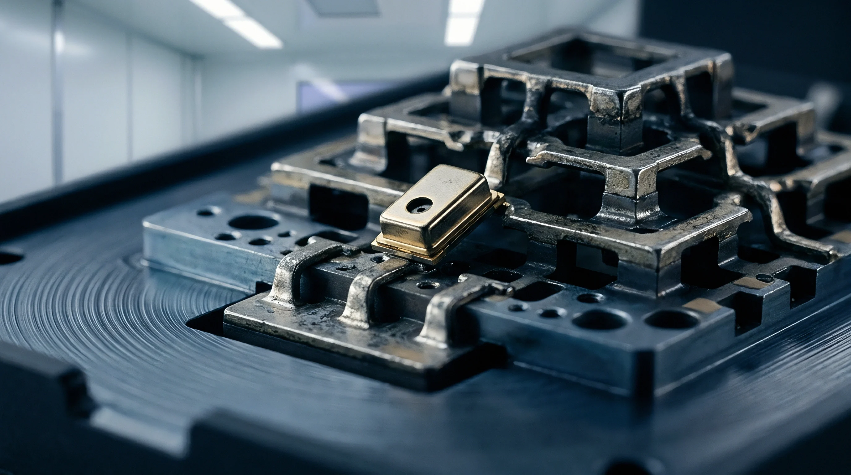
Preventing high-frequency attenuation shifts caused by surface oxidation requires strict engineering control over demountable contact materials, plating thickness, and mechanical contact geometry. Material selection determines the long-term chemical stability and electrical performance of demountable interfaces in harsh operational environments.

Metallurgical Selection for RF Demountable Contacts
Base contact materials must combine high electrical conductivity with mechanical spring resilience. Beryllium-copper and phosphor-bronze serve as standard base alloys. Noble metal plating finishes protect these base substrates from direct atmospheric exposure.
Gold flash coatings measuring less than 0.1 micrometers thick offer insufficient protection against oxygen diffusion. Base substrate nickel underplates migrate through thin gold pores, forming surface nickel oxides. High-reliability RF interfaces specify hard gold plating, alloyed with cobalt or nickel, with a minimum thickness of 0.76 micrometers (30 microinches) placed over a dense, low-porosity nickel underplate measuring at least 2.5 micrometers thick.
Corrosion-resistant noble metal platings shield the substrate underneath.
Alternative plating systems, such as electrolytic palladium-nickel alloy covered by a thin gold hard-cap, deliver high wear resistance and thermal stability while resisting noble metal pore corrosion during long-term field exposure.

Wiping Force and Mechanical Contact Mechanics
Mechanical connector design influences long-term interface resistance by physically disrupting developing surface oxide films during mating operations. Contact normal force and mechanical wiping action represent key mechanical mitigation factors.
A high wiping force mechanically removes surface passivation layers during initial mating.
Spring contacts engineered with a defined wiping motion slide across the opposing contact surface during insertion, mechanically shearing brittle surface oxide films and exposing fresh metal a-spots. Connector specifications must require a minimum normal contact force of 0.3 Newtons per contact point to maintain stable metallic contact under mechanical shock and thermal expansion.
Sufficient normal force prevents momentary contact chatter under dynamic mechanical loads.
Exposed contact interfaces steadily accumulate surface oxidation over time.
Ambient thermal cycling accelerates this surface film growth.

Drafting Sourcing Specifications and RFQ Clauses
Procurement documents for RF modules, pogo-pin test sockets, and coaxial board-to-board connectors must explicitly define metallurgical quality controls and environmental testing requirements. Relying on basic commercial catalog claims leaves products vulnerable to cost-reduced thin flash plating substitutions.
Component procurement contracts specify compliance with EIA-364-23 dry-circuit resistance thresholds alongside post-environmental exposure attenuation limits. Specifications require suppliers to deliver certified X-ray fluorescence plating thickness measurement reports for every manufacturing lot, verifying nickel underplate and outer noble metal layer compliance prior to lot acceptance.
Engineering procurement specifications state that demountable RF interconnect components must maintain less than 0.5 dB insertion loss shift at maximum operational frequency following 200 hours of ASTM B845 Method 2 mixed flowing gas testing, automatically rejecting non-compliant production lots at supplier expense.