Sub-GHz Transceiver Crystal Drive Level Dependency Mitigation via Oxide Passivation
Atomic layer oxide passivation on sub-GHz transceiver crystals eliminates low-drive resistance spikes, preventing oscillator startup stalls and link margin loss.

Blank
Sub-gigahertz transceivers rely on quartz crystal resonators to establish narrow-band channel spacing and synthesize carriers. In low-power radios at 868 MHz and 915 MHz, modern transceivers scale back crystal oscillator drive current during sleep-to-wake transitions to conserve microamperes. Once excitation power drops into the sub-microwatt range, surface characteristics of the quartz blank begin to dominate electromechanical performance.
Standard AT-cut plates ~ processed by wire sawing, lapping, and chemical etching ~ carry surface micro-asperities and localized lattice defects across the active acoustic zone. These microscopic imperfections introduce non-linear damping, creating drive level dependency (DLD).
At nominal drive levels around 100 microwatts, acoustic energy easily overcomes localized surface trap states. Equivalent series resistance (ESR) stays flat, and resonance frequencies behave predictably. Drop the power to 100 nanowatts or below, however, and mechanical displacement amplitudes fall to sub-angstrom scales.
At that scale, energy absorbed by surface dislocations, micro-fissures, and unpassivated dangling bonds represents a large fraction of the total acoustic energy in the plate. The crystal responds with a severe jump in ESR ~ often from 25 ohms to several hundred ohms ~ along with carrier frequency shifts exceeding 10 parts per million (ppm).
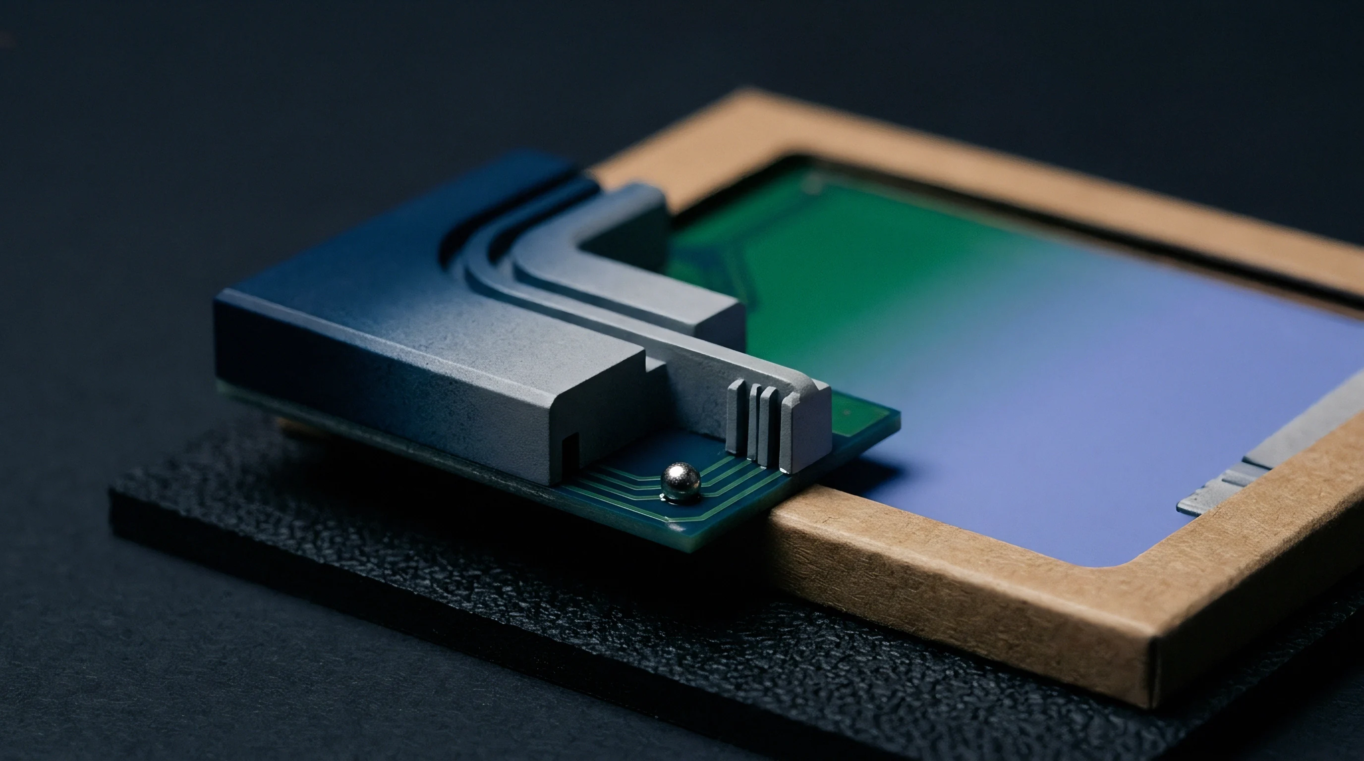
AT Cut Quartz Surface Morphology and Crystal Resonance
Precision quartz plates operate in thickness-shear mode to generate their reference frequencies. Piezoelectric displacement produces high mechanical stress directly beneath the metal electrode boundary, which then tapers toward the unplated outer quartz margins. Standard chemical etching leaves behind broken silica bonds and atomic-scale roughness.
These unbonded silicon and oxygen atoms serve as adsorption sites for ambient moisture, hydrocarbons, and outgassed package contaminants during hermetic sealing. Under weak excitation, the resulting surface states form energy barriers that perturb shear-mode motion.
Acoustic waves propagating across an unpassivated quartz surface scatter against these dense defect fields. At higher drive levels, the mechanical forces simply shove dislocations through their pinning sites, keeping motional resistance low. Below a microwatt, acoustic stress cannot reach the depinning threshold, and energy remains trapped in localized lattice distortions.
This electromechanical loss shows up as a steep increase in effective motional resistance, compromising clock startup in the transceiver.
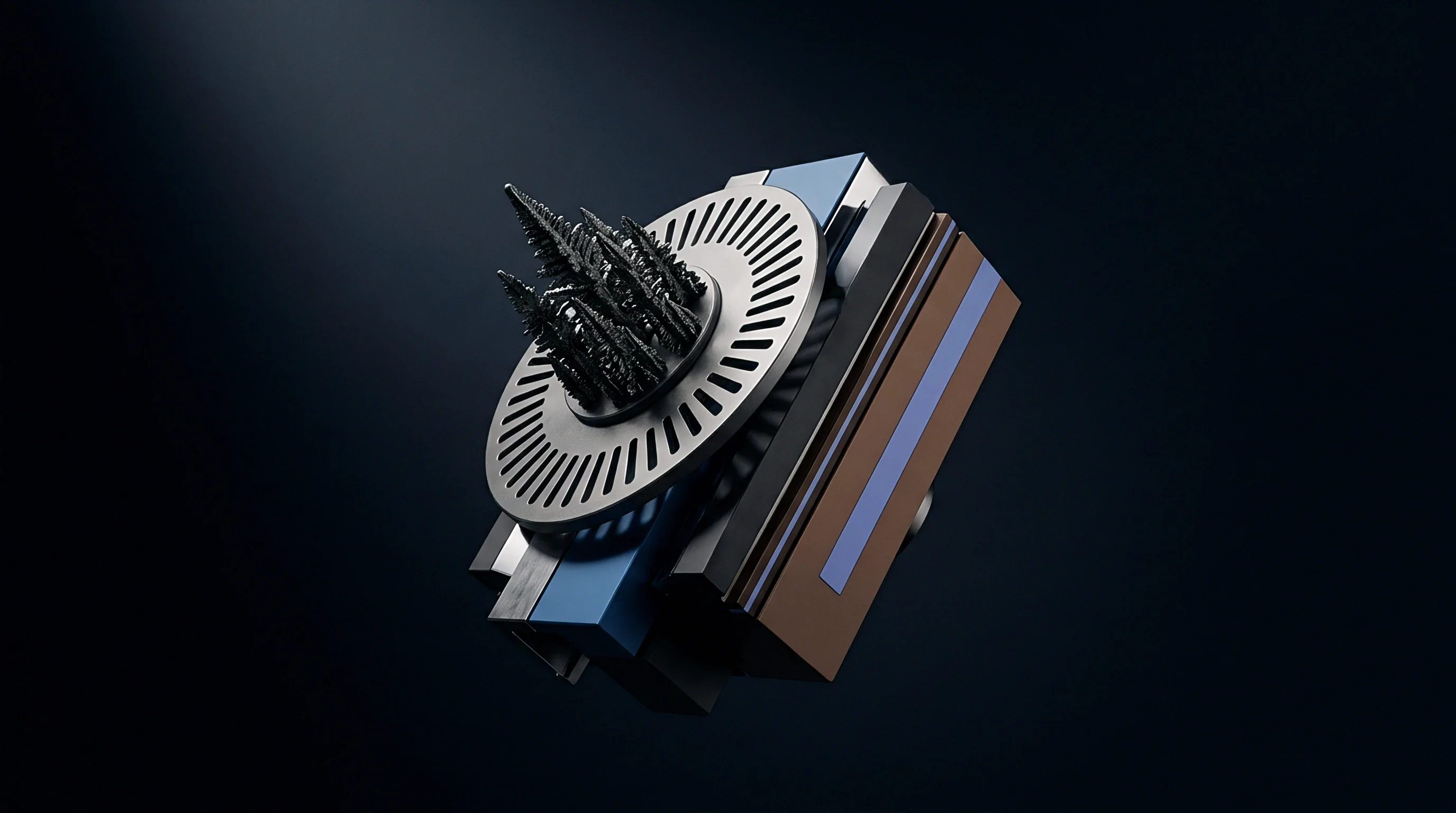
Micro Asperities and Dislocation Pinning Mechanics
Mechanical polishing and chemical etching leave strain fields and micro-asperities concentrated around the plate periphery and the edges of the electrodes. These micro-asperities act as non-linear dampers. Under mechanical strain, dislocations glide through the quartz lattice until they snag on micro-cracks or chemical impurities, pinning them in place.
The oscillator drive circuit must provide enough dynamic current to break through this initial drag. If the transconductance of a sub-gigahertz oscillator lacks the margin to overcome the elevated ESR, the crystal fails to start entirely. The transceiver remains stuck in an un-oscillating state, burning continuous bias current while providing no reference clock.
- Non-starting Pierce Oscillator occurs when low-drive ESR exceeds the negative resistance produced by transceiver oscillator circuitry, preventing startup during fast wake cycles.
- Frequency Offset Jumps surface when crystal drive levels drop during low-power listen modes, pulling carrier frequencies out of receiver channel bandwidth filter limits.
- Extended Startup Latency lengthens wake durations from tens of microseconds to several milliseconds, draining battery capacity during idle channel assessments.
- Intermittent Lock Losses happen when drive level fluctuations trigger phase noise degradation in transceiver phase-locked loops during transmission bursts.
Drive level dependency shifts the equivalent series resistance of a 32 MHz crystal from 25 ohms at 100 microwatts up to 280 ohms when drive power drops below 500 nanowatts.
Using unpassivated, DLD-prone crystals in sub-gigahertz hardware leads directly to field failures in battery-powered networks. Surface instabilities under shifting drive conditions degrade link margins, raise wake energy draw, and trigger intermittent packet losses during low-power polling windows.

Excitation
To cut quiescent battery drain, ultra-low-power radios reduce drive levels to the crystal during sleep-wake transitions. Transceiver chipsets throttle the current fed to the external resonator via register settings or automatic internal gain loops. While running at reduced drive prolongs battery life in duty-cycled sensor nodes, it also forces the crystal to run right where its physical behavior is least predictable.
Drive level dependency is distinctly non-linear across excitation ranges. Between 10 microwatts and 100 microwatts, the resonator tracks classic linear piezoelectric models, maintaining constant motional capacitance and a flat ESR. Below 1 microwatt, surface physics take over: microscopic friction at crystal defects increases effective damping, driving up resistance non-linearly as drive current falls.

Pierce Oscillator Loop Gain and Drive Level Non Linearities
Most transceivers employ an internal single-inverter Pierce oscillator. For dependable startup, the negative resistance generated by the active stage must exceed the crystal ESR by a factor between three and five. This is captured by the gain margin relationship:
Gain Margin = |-R_neg| / ESR_max
If low drive power causes peak ESR to surge from 30 ohms to 300 ohms, an oscillator design providing 150 ohms of negative resistance drops below unity loop gain. Oscillation cannot build up, and the system clock stalls.
The table below tracks crystal drive power, ESR surge values, and resulting gain margins for a standard 32 MHz sub-gigahertz reference design.
| Drive Level (nW) | Unpassivated ESR (Ω) | Passivated ESR (Ω) | Inverter R_neg (Ω) | Unpassivated Margin | Passivated Margin |
|---|---|---|---|---|---|
| 100,000 | 22.5 | 21.0 | 250.0 | 11.11 | 11.90 |
| 10,000 | 28.0 | 22.5 | 250.0 | 8.92 | 11.11 |
| 1,000 | 65.0 | 24.0 | 250.0 | 3.84 | 10.41 |
| 500 | 140.0 | 26.5 | 250.0 | 1.78 | 9.43 |
| 100 | 310.0 | 29.0 | 250.0 | 0.80 | 8.62 |
| 10 | 480.0 | 32.0 | 250.0 | 0.52 | 7.81 |

Could Surface Passivation Mitigate Crystal Resistance Jumps?
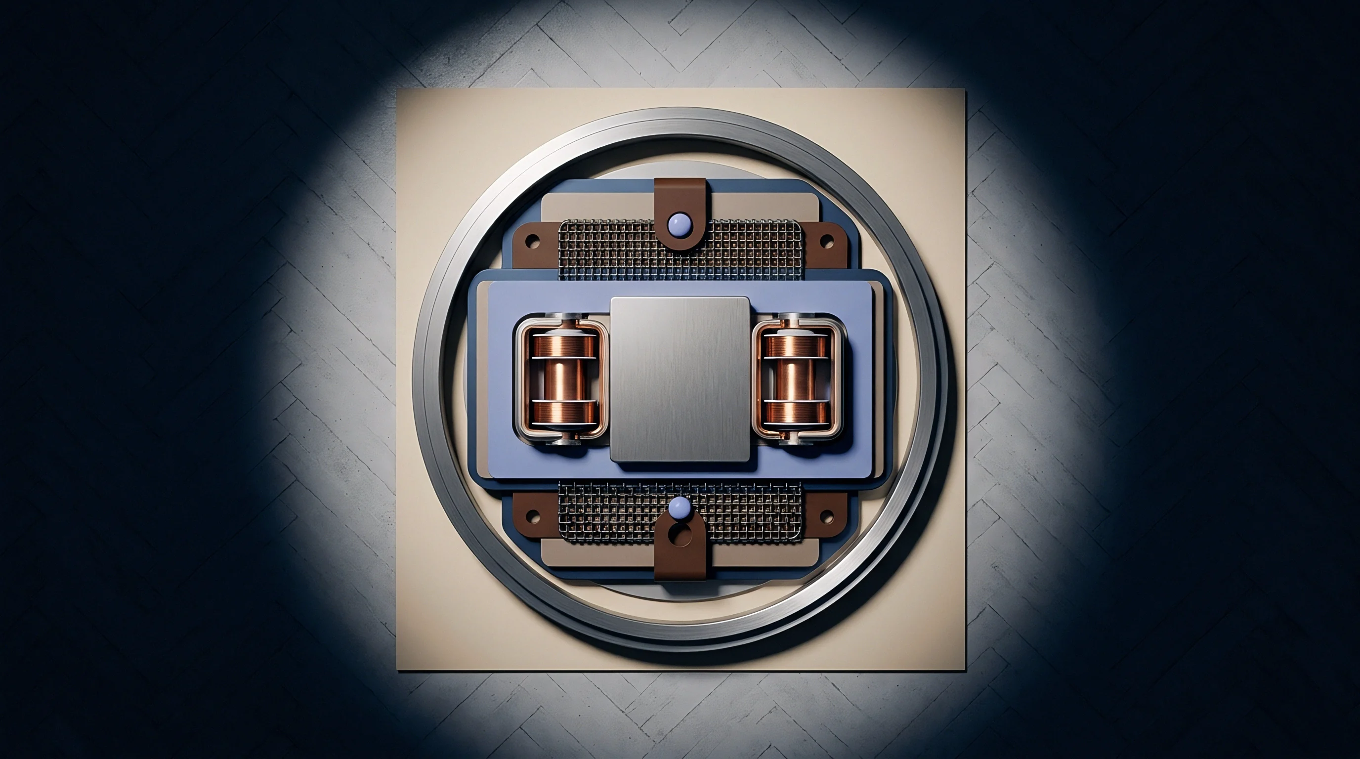
Applying a thin dielectric passivation layer across the bare quartz blank and its metal electrodes targets the exact physical mechanisms behind DLD. Amorphous silicon dioxide (SiO2) or aluminum oxide (Al2O3) films cap microscopic fissures, satisfy dangling surface bonds, and lock down surface contaminants. This keeps ambient moisture and volatile organics from forming weak bonds along active shear paths, preventing excess energy loss even at drive levels down to 10 nanowatts.
By mitigating surface friction and dislocation movement, passivated resonators maintain a steady ESR profile across four orders of magnitude of drive power. The transceiver maintains comfortable gain margin during low-current polling, avoiding oscillator stalls and shortening startup settle times.
Elevated DLD resistance spikes were historically attributed to unwashed organic solvent residues left during package hermetic sealing, leading circuit designers to increase oscillator drive currents rather than alter blank surface chemistry.

Deposition
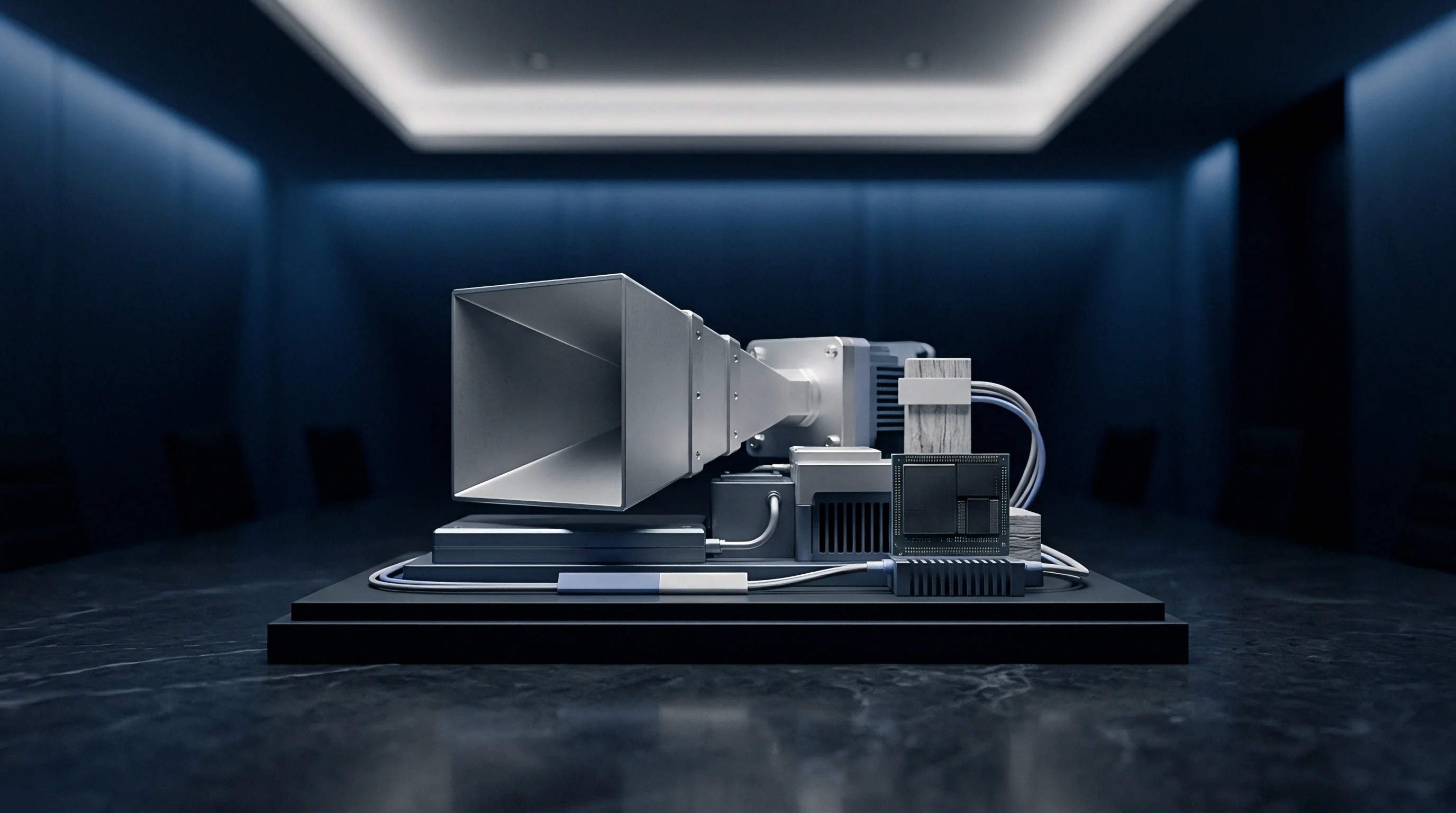
Vapor deposition methods apply dielectric passivation layers directly to quartz blanks to terminate active surface bonds. Atomic Layer Deposition (ALD) and Plasma-Enhanced Chemical Vapor Deposition (PECVD) represent the two primary routes for growing thin oxide films on processed quartz wafers. ALD in particular yields atomic-level thickness control, wrapping conformally over micro-asperities, plate bevels, and electrode steps.
Process parameters require precise control to avoid introducing residual stress into the quartz wafer. Excessive film stress shifts the thickness-shear frequency and warps the temperature coefficient curve. Balancing deposition temperature, precursor dosing, and plasma power produces an amorphous barrier that passivates surface states without damping acoustic resonance.
Atomic Layer Passivation versus Plasma Enhanced Chemical Methods
ALD operates via sequential, self-terminating chemical reactions. Alternating precursor doses ~ such as trimethylaluminum and water vapor for Al2O3 films ~ build the oxide layer by atomic layer. This self-limiting growth leaves zero pinholes and produces uniform film thickness across deeply etched surface features.
PECVD relies on RF plasma to dissociate precursor gases such as silane and nitrous oxide at lower substrate temperatures, depositing silicon dioxide rapidly. However, its step coverage across micro-scale roughness falls short of ALD. Voids and density variations in PECVD films can also trap charge, causing slight electric-field hysteresis under stronger RF excitation.
- Clean raw AT-cut quartz blanks in piranha solution to dissolve residual organic contaminants and remove native surface debris.
- Rinse blanks in ultra-pure deionized water until effluent resistivity reaches 18.2 megohm-centimeters.
- Transfer cleaned quartz wafers into a low-pressure ALD reactor chamber stabilized at 150 degrees Celsius.
- Expose wafers to trimethylaluminum vapor pulses for 150 milliseconds to form a saturated precursor monolayer.
- Purge chamber with high-purity nitrogen gas for 5 seconds to clear unreacted precursor molecules.
- Inject water vapor pulses for 150 milliseconds to hydrolyze the surface monolayer and create dense oxide bonds.
- Repeat the precursor-purge-reactant-purge cycle for 80 iterations to achieve a targeted 10-nanometer film thickness.
- Deposit metallic electrode patterns through shadow masking using electron-beam evaporation.
Interfacial Stress and Quartz Resonance Frequency Tuning
Adding a passivation layer to ultra-thin quartz blanks changes their fundamental thickness-shear resonance. Added mass and residual interfacial stress pull the natural frequency below that of the unpassivated blank. This mass loading is calculated via the Sauerbrey equation:
Δf = – (2 f0^2 Δm) / (A sqrt(ρq μq))
Here, f0 is the fundamental resonant frequency, Δm is the deposited mass, A is the active vibrating area, ρq is the density of quartz (2.648 g/cm³), and μq represents the shear modulus of AT-cut quartz (2.947 x 10^11 g/cm·s²).
A 10-nanometer film of aluminum oxide lowers a 32 MHz fundamental frequency by roughly 450 ppm. Resonator fabricators account for this loading by slightly under-etching raw blanks before coating, ensuring final passivated parts land within standard ±10 ppm manufacturing tolerances.
Standard quartz specification clauses specifying a maximum drive level dependency resistance ratio of 1.3 prevent transceiver oscillator startup failures in low-power duty-cycled radios.
Procurement specifications for reliable sub-gigahertz transceivers enforce the IEC 60444-6 drive level dependency standard. Purchase agreements mandate an ESR ratio (ESR_max / ESR_nominal) under 1.3 across the full span from 10 nanowatts to 100 microwatts, ensuring incoming passivated crystal lots run without issue in low-power transceivers.

Hysteresis
Frequency and equivalent series resistance trace different paths depending on whether drive power is ramping up or ramping down. In unpassivated crystals, this DLD hysteresis loop stems from dynamic gas adsorption and desorption on the exposed quartz surface. As drive power climbs, local acoustic displacement and heating strip off volatile molecules, dropping resistance.
As drive levels fall back down, package ambient molecules rebind to high-energy surface sites, creating a delayed, path-dependent recovery of crystal motional parameters.
This hysteresis disrupts synthesizer channel tracking. In duty-cycled radios, jumping rapidly from transmit drive to low-power sleep pulls reference clocks by several parts per million. That transient frequency pull distorts modulation fidelity in narrow-band frequency shift keying (FSK) and LoRa transmissions.

Surface Traps and Adsorption Desorption Cycles
Bare quartz surfaces present reactive lattice faces that continuously exchange gas molecules with the internal package atmosphere. Physical adsorption traps gas in the micro-valleys of surface roughness. At low drive, these trapped molecules add localized mass and acoustic damping, pulling down the resonator quality factor (Q).
When drive power increases, shear velocity produces enough momentum to break the weak Van der Waals bonds holding these contaminants. Stripped molecules return to the internal package volume, reducing acoustic drag and dropping ESR. When power ramps down, molecules readsorb onto surface asperities.
The resulting loop creates unpredictable clock startup and tuning during rapid listen intervals.
Oxide Barrier Blockade of Hydrocarbon Contamination
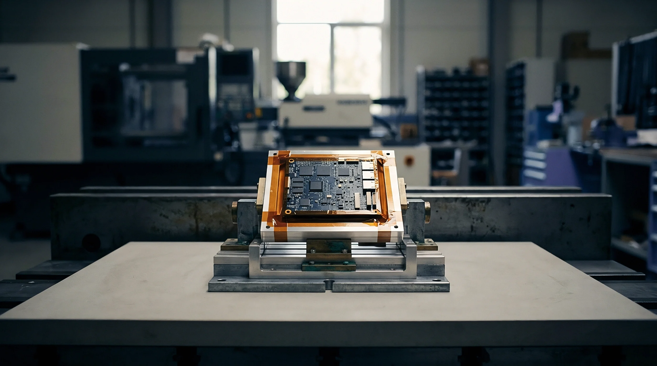
Sealing the blank with an inert dielectric film removes high-energy adsorption sites. The dense network of ALD-deposited silicon dioxide or aluminum oxide provides a solid barrier, preventing gas molecules and trace hydrocarbons from reaching the underlying quartz crystal.
The table below compares drive level hysteresis, peak ESR spikes, and frequency loop widths across untreated, PECVD-coated, and ALD-passivated 32 MHz AT-cut crystals.
| Passivation Material | Process Technique | Film Thickness (nm) | Max ESR Spike (Ω) | ESR Hysteresis (%) | Frequency Hysteresis (ppm) |
|---|---|---|---|---|---|
| Unpassivated Bare Quartz | Chemical Etch Only | 0.0 | 345.0 | 38.5 | 8.4 |
| Silicon Dioxide (SiO2) | Standard PECVD | 25.0 | 58.0 | 8.2 | 1.2 |
| Silicon Nitride (Si3N4) | PECVD | 15.0 | 42.0 | 5.4 | 0.9 |
| Aluminum Oxide (Al2O3) | Atomic Layer Deposition | 10.0 | 28.5 | 1.1 | 0.2 |
| Titanium Dioxide (TiO2) | Atomic Layer Deposition | 8.0 | 31.0 | 1.8 | 0.3 |
Passivating quartz blanks with amorphous oxide barriers eliminates energy barriers that promote contaminant migration across active electrode edges.
Whether sustained thermal exposure at 125 degrees Celsius causes long-term structural changes at the ALD-to-electrode interface ~ potentially reintroducing subtle DLD hysteresis over ten-year operating lifespans ~ remains an active qualification concern for industrial wireless meters.


Sweep
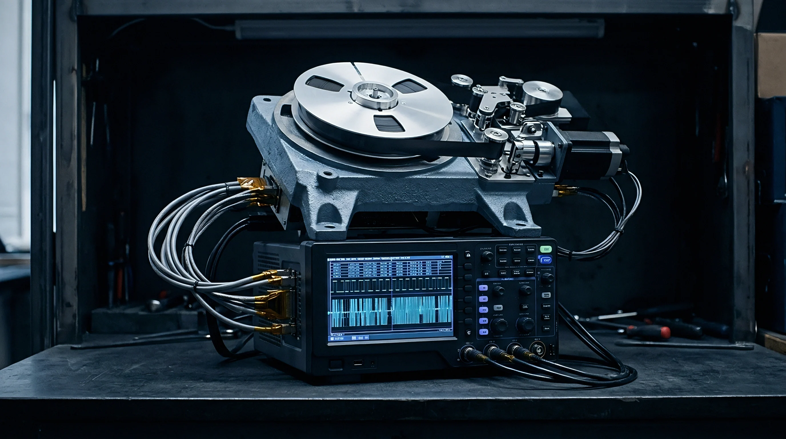
Characterizing crystal drive dependency requires stepping input power from sub-nanowatt regimes up to milliwatt levels. Doing so reliably calls for automated network analyzers or specialized crystal test bridges capable of measuring RF drive currents down into the nanoampere range. These systems record motional resistance, motional capacitance, shunt capacitance, and resonant frequency at every discrete power step.
Sweeping unpassivated crystals from 1 nanowatt to 100 microwatts often reveals narrow, localized ESR spikes known as resistance anomalies. These peaks occur when the primary thickness-shear mode couples into higher-order contour or flexural modes. Oxide passivation dampens this parasitic mode coupling, smoothing the resistance response across the full operating range.

Automated Resistance and Frequency Measurement Protocols
Standard qualification procedures follow the power-sweep framework of IEC 60444-6. Automated instruments increment power logarithmically across at least five decades, pausing at each step for thermal stabilization before sampling impedance. Evaluating parameters on both ascending and descending ramps maps out the hysteresis loop area.
Production screening relies on high-speed spot measurements at critical drive points: typically 10 nanowatts, 1 microwatt, and 100 microwatts. Units showing an ESR ratio over 1.25 or frequency shifts broader than ±2 ppm between low and nominal drive fail factory acceptance checks.
- Maximum Resistance Ratio Limit mandates that peak low-drive ESR divided by nominal high-drive ESR must remain below 1.25 across all production operating temperatures.
- Frequency Shift Ceiling restricts total frequency movement across the complete drive power range to less than ±2.0 ppm to maintain transceiver channel alignment.
- Drive Level Range Verification requires active testing from 10 nanowatts up to 200 microwatts to ensure margin against transceiver oscillator drive variations.
- Thermal Cycling Stability demands that drive level dependency parameters remain within specified tolerances after 500 thermal shock cycles from -40 to +105 degrees Celsius.
Using passivated crystals with linear drive-level profiles ensures dependable oscillator startup without wasting battery power on excessive transceiver bias current.
Budget
Link margins and battery longevity in wireless nodes are tied directly to reference clock startup speed and frequency accuracy. In narrow-band sub-gigahertz radios operating with 12.5 kHz or 25 kHz channel spacing, reference pulling degrades receiver sensitivity. A carrier offset of just 3 kHz caused by drive-induced frequency shifts attenuates the link margin by more than 6 dB, halving working range.
Fast oscillator startup shortens wake periods during routine channel polling. An unpassivated crystal with elevated low-drive ESR can stretch Pierce oscillator wake times from 200 microseconds to beyond 3 milliseconds. In an automated water meter taking readings every ten seconds, that latency wastes hundreds of milliampere-hours per year, significantly shortening service life.
Transceiver Sleep Current and Phase Noise Trade Offs
Devices like the Semtech SX1262 and Texas Instruments CC1312R let designers configure crystal oscillator drive currents. Trimming drive lowers sleep-wake current draw, but eats into negative resistance margin. Passivated crystals permit operating at minimum drive register settings without risking oscillator stalls or frequency pulling.
Consistent crystal parameters at low drive also preserve phase noise performance close to the carrier. Reciprocal mixing between phase noise and adjacent-channel blockers degrades channel selectivity. By keeping resonator Q high across all drive currents, passivated crystals maintain receiver performance in congested radio bands.

Landed Cost Analysis for Passivated Crystal Integration
Adding ALD or PECVD oxide passivation introduces extra fabrication steps, increasing unit component prices. When evaluated at the system level, however, passivated resonators yield net savings by allowing smaller battery capacities, cutting board-level test fallouts, and preventing field returns.
The model below compares performance, power draw, and costs across three crystal options deployed in a 915 MHz smart grid endpoint.
| Parameter | Standard Bare Quartz | PECVD SiO2 Passivated | ALD Al2O3 Passivated |
|---|---|---|---|
| Unit Component Cost (USD) | 0.18 | 0.26 | 0.34 |
| Startup Latency at Low Drive (μs) | 2800 | 450 | 180 |
| Low-Drive ESR Max (Ω) | 320.0 | 48.0 | 26.5 |
| Frequency Pulling Error (ppm) | ±8.5 | ±1.2 | ±0.3 |
| Link Margin Degradation (dB) | 5.2 | 0.8 | 0.1 |
| Estimated 10-Year Field Return Rate (%) | 2.40 | 0.15 | 0.02 |
| Annualized Node Battery Draw (mAh) | 182.0 | 124.0 | 112.0 |
Unpassivated crystal resonators subject to duty-cycled operation exhibit frequency drifts that degrade channel selectivity in narrowband Sub-GHz links.
Specifying atomic layer passivated crystals reduces total bill-of-materials cost by trimming required battery sizing. Over a production run of 500,000 sub-gigahertz utility meters, choosing ALD-passivated 32 MHz crystals adds 80,000 USD in component costs. However, downsizing the battery from 2600 mAh to 1900 mAh saves 350,000 USD in cell procurement, netting 270,000 USD in direct savings while lowering warranty exposure across field deployments.