Nonlinear Quantum Tunneling Conduction Model for Interfacial Oxide Layers in RF Contacts
Interfacial native oxides create non-linear quantum tunneling barriers across RF contacts, generating passive intermodulation that degrades receiver sensitivity.


Film
Bare metal exposed to air grows a self-limiting native oxide film within milliseconds of fabrication. Measuring between 0.5 and 5.0 nanometers thick, these surface layers turn what elementary electromagnetics models as a simple conductor-conductor interface into a metal-insulator-metal barrier. At direct current, this manifests as nothing more than a marginal increase in contact resistance.
In high-power RF transmission paths, however, that same oxide geometry introduces sharp non-ohmic voltage drops. When carrier tones pass through the junction, the non-linear relationship between current density and electric field strength generates passive intermodulation products right in the physical joint.
The initial potential barrier profile across the junction depends directly on the stoichiometry and phase of the interfacial film. Copper exposed to ambient air develops a duplex structure: a dense inner cuprous oxide layer capped with a hydrated cupric oxide film. Aluminum quickly forms an amorphous alumina passivating sheath that blocks further oxygen diffusion once it reaches roughly three nanometers.
Nickel produces a thin, highly stable oxide that resists displacement under light normal loads. Each material system establishes a characteristic energy bandgap, work function offset, and relative permittivity that dictate the electrostatic barrier presented to conduction electrons.
Interfacial native oxides act as asymmetric dielectric barriers across metal contact junctions under ambient atmospheric pressure.
Microscopic surface roughness prevents true planar contact across RF interfaces; mating surfaces touch only at discrete microscopic high points, or asperities. Because of this, the real contact area is tiny compared to the nominal footprint ~ often less than one part in ten thousand under standard clamping loads. At these localized contact spots, mechanical stress deforms the metal, rupturing brittle oxide films to form direct metal-to-metal bridges called a-spots.
Around these metallic bridges lie regions where the oxide remains intact, separated by sub-micron gaps or partially compressed dielectric films.
Current across an RF joint splits between two parallel mechanisms: bulk conduction through metallic a-spots governed by Maxwellian constriction resistance, and secondary conduction through the surrounding thin oxide via quantum mechanical tunneling. When the total area of the unruptured oxide vastly exceeds the aggregate area of the metallic bridges ~ or when fretting corrosion breaks those metallic paths ~ tunneling becomes the dominant mode of high-frequency signal transfer across the interface.
Native Oxide Kinetics at Metallic Interfaces
Atmospheric oxidation begins when electrons transfer from the bulk metal to adsorbed surface oxygen. This charge transfer sets up a localized Mott potential across the growing dielectric layer, creating an electric field that pulls metal cations through the oxide lattice at room temperature. Growth is rapid initially, but as the film thickens and the internal field drops, the reaction slows from logarithmic kinetics to a self-limiting parabolic rate.
Operational humidity and temperature swings alter the stoichiometry of these films over time. Moisture introduces hydroxyl groups into the oxide matrix, depressing the local breakdown voltage and increasing dielectric losses, while accelerating galvanic corrosion across dissimilar metal junctions. These native layers are rarely uniform across a contact spot; crystalline defects, grain boundaries, and micro-voids cause significant local variation in barrier height and layer thickness.
Connector mechanical design largely determines whether these films remain intact during assembly. Slider mechanisms and spring-loaded pogo pins rely on mechanical wipe to shear the fragile oxide skin on engagement, pushing displaced debris to the contact perimeter and exposing bare metal. If the normal force falls below the yield threshold of the base metal, the wipe action fails to clear the film, leaving the joint to rely primarily on tunneling across an unbroken dielectric barrier.

Asperity Deformations and Effective Tunneling Surface
Plastic deformation governs microscopic contact peaks during initial mating. Under an applied normal force, the softest surface asperities yield plastically until the combined real contact area can support the mechanical load. Under the Greenwood-Williamson model, asperity peak heights follow a Gaussian distribution, meaning lower clamping forces leave a large share of interface asperities in elastic contact where the oxide remains completely unbroken.
Calculating the true contact area requires balancing base metal hardness, surface micro-topography, and clamping torque. Under typical connector torque, compressive stresses at asperity peaks easily exceed bulk yield strength. Micro-cracks in the brittle oxide allow the softer underlying metal to extrude through, forming cold-welded micro-junctions.
These direct metal pathways carry low-frequency current with minimal resistance, effectively masking the non-linear tunneling paths that emerge once high-power RF currents are applied.
The distribution of thin oxide regions surrounding these metallic asperities creates an array of parallel tunneling capacitors. Each non-contacting zone functions as a parallel-plate capacitor with a nanometer-scale dielectric gap. Below one gigahertz, the capacitive reactance of these gaps remains high enough to force current through the metallic a-spots.
In the multi-gigahertz range, however, displacement currents through the oxide rise substantially, coupling RF energy directly into the non-linear tunneling channels.
| Base Metal System | Dominant Native Oxide | Self-Limiting Thickness (nm) | Dielectric Constant (r) | Mean Barrier Height (eV) |
|---|---|---|---|---|
| Copper (Cu) | Cu2O / CuO | 1.8 to 3.5 | 7.5 | 0.65 to 0.95 |
| Aluminum (Al) | Al2O3 | 2.5 to 4.5 | 9.3 | 1.80 to 2.40 |
| Nickel (Ni) | NiO | 1.2 to 2.2 | 11.8 | 1.20 to 1.50 |
| Silver (Ag) | Ag2O | 0.8 to 1.5 | 5.6 | 0.45 to 0.70 |
| Brass (Cu-Zn) | ZnO / Cu2O | 2.0 to 4.0 | 8.4 | 1.10 to 1.60 |
Environmental aging degrades the ratio of metallic a-spots to oxide tunneling area. Thermal cycling expands and contracts mismatched metals, generating microscopic fretting motion at the contact interface. This fretting shears existing cold-welded micro-junctions, exposing fresh metal that quickly re-oxidizes.
Over thousands of cycles, metallic a-spots convert into oxidized junctions, turning an initially linear ohmic contact into a non-linear quantum tunneling barrier.
Unmanaged native oxide growth remains a primary cause of intermittent RF degradation in unsealed outdoor wireless systems. Skipping mechanical wipe requirements during connector assembly leaves native dielectric films intact across signal paths, introducing non-linear barrier physics into otherwise well-designed link budgets.


Tunneling
Conduction across ultra-thin interfacial oxide films is governed by quantum mechanics. When the physical thickness of an oxide layer drops below five nanometers, the wavefunctions of conduction electrons in the metal extend through the potential barrier of the insulator. Electrons cross the forbidden gap without the thermal energy required to clear the barrier height.
This quantum tunneling current scales exponentially with barrier thickness and with the square root of the effective barrier height.
Current transport through thin insulating barriers is modeled using the Simmons tunneling formulation. Simmons derived a generalized expression for current density across arbitrary potential profiles by integrating electron transmission probabilities across the Fermi-Dirac distributions of the opposing electrodes. At very low applied voltages, the barrier remains roughly rectangular, producing an ohmic current-voltage relationship.
As the voltage drop across the oxide increases, the barrier tilts into a trapezoid, introducing higher-order non-linear terms into the I-V characteristic.
Image-force lowering reshapes the potential barrier profile. An electron traversing the dielectric induces positive image charges in both metal faces, which rounds off the barrier corners and lowers the potential peak. This correction reduces both the effective thickness and the effective height of the barrier, increasing the calculated tunneling current density by orders of magnitude compared to an ideal rectangular model.
The magnitude of this image-force reduction depends on the relative permittivity of the interfacial oxide.
Simmons Formulation for Thin Dielectric Interlayers
Evaluating quantum tunneling across an oxide junction requires integrating current density across the insulator gap. The Simmons equation models current density J as a function of barrier thickness s, mean barrier height Phi_0, and applied voltage V across the film:
J(V) = (e / (2 pi h s^2)) { (Phi_0 – V/2) exp( -A sqrt(Phi_0 – V/2) ) – (Phi_0 + V/2) exp( -A sqrt(Phi_0 + V/2) ) }
where e is the elementary electron charge, h is Planck’s constant, and the parameter A is given by:
A = (4 pi s sqrt(2 m )) / h
Here, m is the effective electron mass in the oxide conduction band. When the applied voltage V is small relative to the mean barrier height Phi_0, a Taylor series expansion of the Simmons equation around V = 0 yields polynomial coefficients governing small- and large-signal conduction:
J(V) = c_1 V + c_2 V^2 + c_3 V^3 + c_4 V^4 + c_5 V^5 +.
The first-order coefficient c_1 represents the zero-bias linear conductance of the oxide film. The second-order coefficient c_2 stems from structural asymmetry between the electrodes, such as differences in work functions or oxygen concentration gradients across the layer. The third-order coefficient c_3 represents the primary non-linearity in symmetric metal-insulator-metal junctions, acting as the primary physical driver of third-order passive intermodulation in RF systems.
Direct quantum tunneling dominates current conduction across oxide barriers thinner than two nanometers at bias potentials below one volt.
Extracting these non-linear tunneling coefficients involves a step-by-step numerical procedure based on measured contact geometry:
- Determine the effective contact area by converting mechanical normal force and metal yield strength into total micro-asperity surface area.
- Estimate the average oxide film thickness using spectroscopic ellipsometry or contact capacitance measurements taken across trial junctions.
- Calculate the zero-bias barrier height by taking the difference between the metal work function and the electron affinity of the interfacial oxide phase.
- Compute the image-force correction parameter to determine the reduced barrier thickness under applied peak RF electric fields.
- Perform a Taylor series expansion of the image-corrected Simmons equation to extract the explicit third-order coefficient c_3 for target RF carrier power levels.
Elevating the electric field across the oxide triggers a transition in the transport mechanism. When the voltage drop V exceeds the zero-bias barrier height Phi_0 divided by electron charge e, the barrier distorts from a trapezoid into a triangle. The effective barrier width at the electron energy level then narrows linearly with applied voltage, shifting conduction into the Fowler-Nordheim field emission regime, where electrons tunnel directly into the oxide conduction band before reaching the opposing contact.
Field Emission Transitions under High Electric Fields
Field emission introduces severe non-linearity into the contact’s I-V transfer characteristic. In the Fowler-Nordheim regime, current density scales with the square of the electric field strength multiplied by an exponential decay factor:
J_FN(E) = B E^2 exp( – C / E )
where E is the electric field strength (V/s), and B and C are constants derived from effective electron mass and the field emission barrier height. In high-power RF transmission paths, peak voltage swings across asperity gaps can easily drive local fields above one megavolt per centimeter, triggering transient excursions into Fowler-Nordheim emission on every half-cycle of the carrier.
This oscillation between direct tunneling and field emission generates strong higher-order odd terms in the transfer function. While direct tunneling yields predominantly third-order products, field emission injects fifth-, seventh-, and ninth-order mixing components into the path. These higher-order products frequently land in adjacent receiver allocation bands, degrading receiver sensitivity across multi-band systems.
Operating temperature modifies tunneling behavior via Fermi-Dirac thermal broadening. Higher temperatures widen the energy distribution of conduction electrons in the metal, increasing the population of electrons encountering a lower effective barrier near the top of the bandgap. Thermal excitation also enables phonon-assisted tunneling through oxide defects, introducing temperature-dependent shifts in the non-linear coefficients c_2 and c_3.
Localized micro-heating at high-current asperity tips alters the long-term stability of the effective barrier height during continuous multi-carrier transmission.


Distortion
Non-ohmic conduction through interfacial oxides turns passive transmission lines into radio frequency mixers. When two high-power carrier tones at frequencies f_1 and f_2 traverse a contact with cubic I-V non-linearity, the third-order coefficient c_3 mixes these signals, generating intermodulation products at 2 f_1 – f_2 and 2 f_2 – f_1. If these fall inside the receive band of a co-located transceiver, they raise the noise floor, override weak incoming signals, and degrade receiver margins.
Multi-tone excitation across an oxidized joint generates an intermodulation spectrum that scales sharply with carrier power. The fundamental powers P_1 and P_2 dictate third-order intermodulation power P_IM3 according to a 3:1 logarithmic relationship: every 1 dB increase in carrier power increases third-order intermodulation power by 3 dB. A joint showing acceptable intermodulation levels at ten milliwatts can generate crippling interference when carrier power reaches twenty watts.
Interfacial contact distortion directly causes receiver desensitization in multi-carrier cellular, LTE-M, NB-IoT, and sub-GHz deployments. For an LTE-M module on Band 28 (transmit: 703 to 748 MHz, receive: 758 to 803 MHz), two transmit carriers at 710 MHz and 735 MHz generate a third-order mixing product at 760 MHz (2 * 735 – 710 = 760 MHz). This falls squarely in the receive band, lifting the effective noise floor and degrading sensitivity by tens of decibels.
Nonlinear Mixing and Passive Intermodulation Generation
Modeling two-tone passive intermodulation requires passing the contact voltage waveform through the non-linear Simmons current equation. Substituting a two-tone stimulus V(t) = V_1 cos(w_1 t) + V_2 cos(w_2 t) into the cubic transfer function produces expressions for fundamental, harmonic, and intermodulation currents:
I(t) = c_1 + c_3 ^3
Expanding the cubic binomial yields the current amplitude I_IM3 at the 2 w_1 – w_2 intermodulation product:
I_IM3 = (3 / 4) c_3 (V_1^2) V_2
Converting this current into delivered power over a characteristic line impedance Z_0 shows that third-order intermodulation power scales directly with the square of the cubic coefficient c_3. Halving the interfacial oxide non-linearity lowers generated intermodulation power by six decibels.
Observed macro-level passive intermodulation across an RF interface is the phase-coherent sum of hundreds of parallel asperity tunneling junctions. Because asperity gap widths, oxide thicknesses, and barrier heights vary across the mating face, individual tunneling sites generate intermodulation components with different phase offsets. Destructive interference partially suppresses aggregate intermodulation power, but vibration and thermal expansion continuously shift these internal phase relationships, causing intermodulation levels to drift over time.
Four primary physical mechanisms drive this conversion of carrier power into passive intermodulation across an oxidized interface:
- Asymmetric Barrier Inversion occurs when dissimilar metals create an asymmetric potential barrier profile, driving strong second-order and even-harmonic mixing products across the interface.
- Thermal Modulation Dynamics manifest when high RF peak power induces cyclic micro-scale temperature swings at asperity tips, dynamically modulating local oxide barrier height at audio and baseband frequency rates.
- Asperity Breakdown Transients emerge when peak RF voltage spikes momentarily exceed the localized dielectric breakdown threshold of thin oxide pockets, causing abrupt current steps that inject broad-spectrum impulse noise into the transmit path.
- Micro-Arcing Excursions develop across sub-nanometer air gaps separating non-contacting oxide islands, producing localized plasma discharges under high transmit power levels.

Why Does Carrier Spacing Exacerbate Nonlinear Contact Interference?
Narrowing the frequency separation between transmit carriers pulls higher-order intermodulation products closer to the active channel edges. When carrier spacing drops below one megahertz, high-order products like fifth-order (3 f_1 – 2 f_2) and seventh-order (4 f_1 – 3 f_2) land directly inside internal receiver passbands. Fixed-cavity duplexers that filter out far-off spurious emissions offer no attenuation against near-in intermodulation generated downstream, such as in antenna switches, pogo pin arrays, or board-to-board connectors.
OFDM-based digital protocols, including Wi-Fi 6E, 5G NR, and multi-carrier cellular, compound these contact non-linearities. An OFDM signal combines hundreds of densely spaced subcarriers, resulting in high peak-to-average power ratios (PAPR). When peak voltage swings hit an oxidized contact, the instantaneous electric field pushes tunneling barriers deep into non-linear regimes, producing spectral regrowth that elevates the noise floor across the entire channel rather than generating isolated spurs.
High RF carrier power exponentially increases third-order intermodulation products generated within non-ohmic interfacial junction barriers.
| Radio Protocol | Transmit Band (MHz) | Receive Band (MHz) | Target Carrier Power (dBm) | Typical Desense (dB) |
|---|---|---|---|---|
| LTE-M (Band 28) | 703 to 748 | 758 to 803 | +23.0 | 12.5 to 28.0 |
| NB-IoT (Band 20) | 832 to 862 | 791 to 821 | +23.0 | 8.0 to 19.5 |
| LoRaWAN (US915) | 902 to 915 | 923 to 928 | +30.0 | 14.0 to 32.0 |
| Wi-Fi 6 (2.4 GHz) | 2400 to 2483.5 | 2400 to 2483.5 | +20.0 | 4.5 to 11.0 |
| 5G NR (n78 sub-6G) | 3300 to 3800 | 3300 to 3800 | +26.0 | 6.0 to 22.0 |
Sub-GHz industrial systems are especially vulnerable to contact non-linearities. Long-range links using LoRaWAN or proprietary sub-GHz radios operate close to the thermal noise floor, relying on high receiver sensitivity (down to -137 dBm) to maintain connectivity over long distances. An oxidized connector pin producing even a modest -110 dBm third-order product will degrade receiver sensitivity by twenty-seven decibels, cutting practical coverage by more than eighty percent.
Single-tone S-parameter sweeps on a vector network analyzer fail to capture contact oxidation because they run at low power (typically -10 dBm), operating entirely within the linear, zero-bias regime of the tunneling barrier. A connector can pass S-parameter qualification without difficulty yet produce severe intermodulation distortion under multi-tone, high-power excitation.


Metrology
Isolating tunneling parameters in physical RF contacts requires test benches that can detect microvolt-level non-linearities under high carrier power. Standard DC milliohm meters use low-current pulses that either fail to break through surface oxides or apply enough voltage to puncture thin films, modifying the joint during measurement. Proper characterization requires dynamic non-linear V-I curve fitting paired with high-dynamic-range passive intermodulation spectrum analysis.
Direct measurement of tunneling barrier parameters relies on swept small-signal harmonic detection. By applying an ultra-low-distortion sinusoidal current I(t) = I_0 sin(w t) across the contact and capturing the third-harmonic voltage V_3w with a lock-in amplifier, the cubic non-linear coefficient c_3 can be calculated directly. Sweeping this harmonic measurement across DC bias voltages maps the derivative of conduction density, providing a profile of mean barrier height Phi_0 and film thickness s.
High-power intermodulation metrology validates contact linearity under realistic operating conditions. Following IEC 62037, two continuous-wave tones at +43 dBm (20 Watts) per tone are applied to the device under test while monitoring generated intermodulation products with a high-dynamic-range receiver. The test bench itself must maintain a residual background floor below -130 dBm (-173 dBc) so that fixture-generated distortion does not obscure subtle contact non-linearities.

Low Level Harmonic Extraction and Sweep Dynamics
Harmonic extraction separates non-ohmic tunneling from bulk heating. As a metal warms, its resistance increases linearly with temperature, shifting symmetrical voltage traces up or down without harmonic conversion. Quantum tunneling non-linearities, by contrast, create an instantaneous, phase-locked distortion response that tracks the RF voltage waveform without thermal lag well into the tens of gigahertz.
Accurate coefficient measurement requires strict source isolation. Low-pass and band-pass cavity filters placed after the power amplifiers strip transmitter harmonics before the carriers reach the test interface. Impedance mismatches between the amplifier and contact fixture generate standing waves, distorting peak voltage swings across the barrier.
High-power ferrite circulators and precision directional couplers in the launch line stabilize power delivery into non-linear contact interfaces.
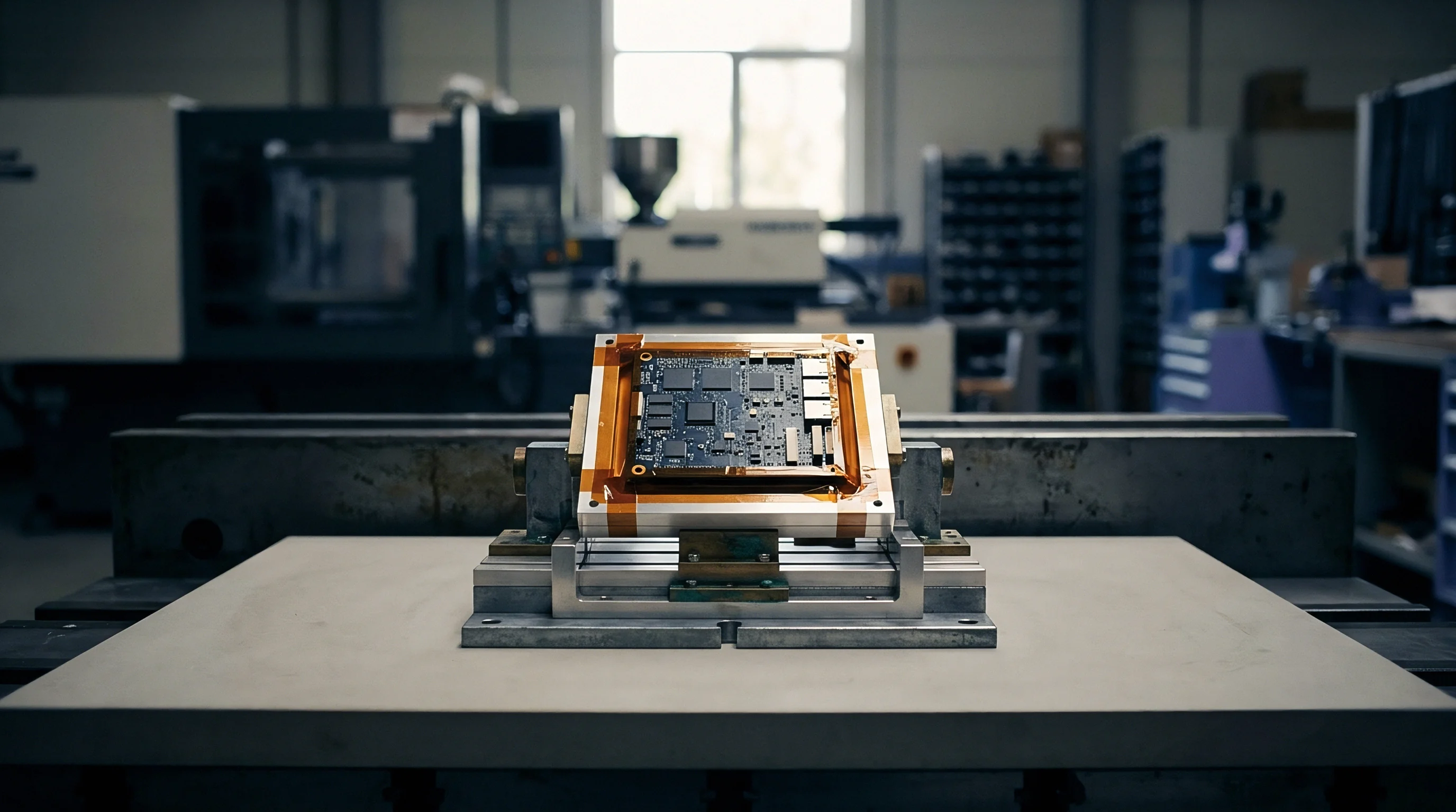
Vibration during intermodulation sweeps helps identify dynamic oxide breakdown. Mounting the test fixture on a multi-axis electrodynamic shaker while recording PIM3 spectral lines reveals contact stability under mechanical stress. Solid metallic micro-junctions exhibit stable intermodulation levels under vibration, whereas joints suffering from fretting show abrupt 20-40 dB spikes as a-spots fracture and re-form under shear.
Parameter Fitting for Potential Barrier Identification
Extracting physical oxide parameters from measured third-harmonic coefficients c_3 and linear resistance c_1 requires non-linear least-squares fitting against the Simmons model. The solver iterates across values of barrier height Phi_0, thickness s, and real contact area A_r until modeled current curves match measured multi-tone intermodulation levels across carrier power steps.
Fitting accuracy depends on accounting for image-force barrier lowering. Ignoring image charge dynamics can lead to overestimating oxide thickness by up to thirty percent while underestimating barrier height. Including the dielectric constant epsilon_r of the specific metal oxide phase in the iteration loop stabilizes the solver, yielding physical dimensions consistent with cross-sectional transmission electron microscopy (TEM) scans.
Evaluating contact integrity across incoming module lots involves running automated two-tone sweeps from +20 dBm to +43 dBm per carrier. Plotting intermodulation power against carrier power on a log-log scale produces an empirical scaling slope. Linear contacts generate no detectable distortion above the -130 dBm bench floor; oxide barriers show a characteristic 3:1 logarithmic slope, while micro-arcing across damaged plating layers produces steep, irregular slopes exceeding 5:1.
Reliable characterization of interfacial contact oxides follows a defined evaluation sequence:
- Small-Signal Linearity Bounds must be established by sweeping direct-current bias from -100 mV to +100 mV while recording differential conductance to confirm zero-bias ohmic limits.
- Carrier Power Scaling Factor calculation requires stepping two-tone RF power across a minimum 20 dB dynamic range to verify theoretical 3:1 intermodulation slope behavior.
- Temperature Dependency Drift evaluation involves heating the contact fixture from -40 to +85 degrees Celsius to separate Fermi-Dirac thermal broadening from mechanical thermal relaxation.
- Mechanical Load Correlation testing demands recording PIM3 values continuously while stepping normal force from zero to maximum mechanical specification limits.
Section 4.2 of IEC 62037 mandates two transmitter tones at forty-three decibels milliwatt to expose non-ohmic interfacial contact junctions.
Identical nominal plating specifications can show a 14 dB spread in third-order intermodulation performance, exposing the limitations of standard direct-current resistance checks in detecting sub-nanometer native oxide layers across RF transmission interfaces.
Procurement specifications for high-reliability RF interconnects often enforce intermodulation limits measured under dynamic vibration. Section 4.2 of IEC 62037 specifies two +43 dBm tones, requiring third-order intermodulation products to remain below -155 dBc across operating temperatures. Meeting this threshold requires strict supplier quality controls, optimized plating stacks, and noble metal surface treatments.


Plating
Preventing quantum tunneling conduction across RF contacts requires engineering the mating interface to inhibit native oxide formation. Noble metal surface finishes provide primary protection against oxidation; gold, silver, and platinum-group metals have high standard reduction potentials and resist spontaneous oxygen reaction under atmospheric conditions. Choosing the right plating architecture, barrier underlayers, and mechanical normal forces ensures long-term passive linearity across field deployments.
Gold plating is widely used for low-level signal contacts because it does not oxidize in air, maintaining clean metallic contact under low mating forces. Hard gold alloys with cobalt or nickel additions improve wear resistance but introduce minor ferromagnetic non-linearities at high power levels. Soft gold over sulfamate nickel delivers lower distortion, provided the gold layer is thick enough to eliminate pinhole porosity that allows oxygen to reach the underlying base metal.
Silver plating provides excellent conductivity and intermodulation performance in high-power RF systems. Although silver reacts with ambient sulfur to form silver sulfide, silver oxide remains thermodynamically unstable under normal conditions and breaks down under light contact loads. Silver sulfide films have low barrier heights (below 0.5 eV) and break down electrically at very low voltages, preventing the formation of stable tunneling barriers across high-power coaxial joints.

Metallurgical Barrier Systems for Passive Linearity
Multi-layer plating stacks prevent base metal atoms from diffusing to the surface to form oxides. Copper-based alloys require a dense underplate barrier before noble topcoat deposition; applying gold directly over copper fails because copper atoms diffuse through gold grain boundaries at room temperature, forming copper oxide on the surface within weeks.
Nickel underplating serves as a reliable diffusion barrier and provides a firm mechanical backing for noble topcoats. Electrolytic sulfamate nickel produces low-stress deposits well-suited for flexible contact springs. Electroless nickel-phosphorus yields uniform coverage on complex geometries, but deposits with phosphorus content below eight percent exhibit ferromagnetic non-linearities.
High-phosphorus electroless nickel remains non-magnetic, balancing diffusion resistance with low intermodulation distortion.
Tri-metal alloy plating (copper, tin, and zinc, often sold as white bronze or Sucopro) provides a non-magnetic alternative to nickel underlayers in high-power RF connectors. Tri-metal matches the non-magnetic performance of silver while providing solid corrosion resistance and low distortion. Capping a tri-metal underlayer with a thin gold or silver flash protects against both surface oxidation and magnetic mixing products.
Mechanical Wipe Mechanics and Normal Force Ceilings
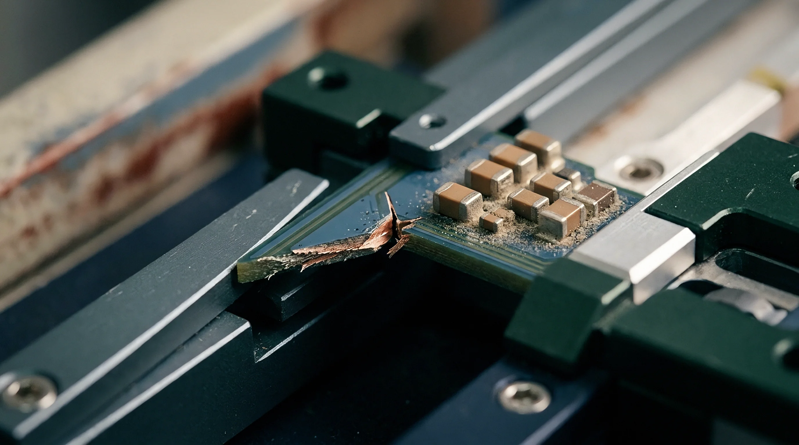
Mechanical design dictates whether a contact operates via linear metallic conduction or non-linear tunneling. A high initial normal force ensures that microscopic asperity tips puncture native oxide films during mating. A minimum normal force of 100 grams-force (0.98 Newtons) per contact point deforms the base metal plastically, creating metallic a-spots that bypass tunneling paths.
Wipe distance determines how effectively mating pins clear surface contamination. Designing contact springs for at least 0.25 millimeters of wipe shears native oxides and clears debris away from the primary electrical contact zone. Stiff spring profiles help preserve normal force over the connector’s operating life, resisting thermal stress relaxation that could otherwise reduce clamping force and allow oxide growth to encroach on bare a-spots.
| Plating Stack-up Architecture | Top Layer Thickness (um) | Underlayer System | Typical Residual PIM3 (dBc @ 2×43 dBm) | Oxide Tunneling Risk Profile |
|---|---|---|---|---|
| Hard Gold over Sulfamate Nickel | 0.76 to 1.27 | 2.54 um Nickel | -150 to -158 | Low (Porous pinholes in thin gold) |
| Soft Gold over High-P Ni | 1.27 to 2.54 | 3.81 um Ni-P (10% P) | -162 to -168 | Negligible (Barrier migration sealed) |
| Silver over Tri-Metal Alloy | 3.00 to 5.00 | 2.00 um Cu-Zn-Sn | -166 to -172 | Very Low (Sulfide breaks easily) |
| Flash Gold over Brass (Direct) | 0.10 to 0.25 | None | -115 to -132 | Severe (Rapid Cu/Zn diffusion) |
| Tin over Copper (Matte Tin) | 3.00 to 7.00 | 1.27 um Copper | -125 to -140 | High (Thick oxide growth under air) |
Environmental sealing shields contact interfaces from moisture, airborne pollutants, and salt spray. Integrating fluorosilicone or EPDM O-rings into connector shells prevents oxygen ingress into the mated cavity. Unsealed outdoor connectors face accelerated oxidation from humidity and thermal cycling, introducing non-linear tunneling distortion long before an open-circuit failure occurs.
Using heavy silver or gold over non-magnetic underlayers preserves RF linearity across harsh operating environments. High contact normal forces combined with adequate wipe action consistently cut through native oxide films, keeping passive intermodulation low and protecting receiver sensitivity.