Meaning
Physical conductor pathways designed for signals above thirty gigahertz require rigorous electromagnetic boundary confinement to control reflection and transmission losses across module integration boundaries. Transmission line structures classified as millimeter wave interconnects route multi-gigabit data streams and high-frequency wireless carriers between integrated circuits, substrate boards and antenna elements. These structures maintain strict physical dimensions to suppress parasitic surface modes, prevent spatial radiation and deliver controlled characteristic impedance.
Their functional domain ends where electromagnetic energy transitions into free space via an antenna or enters an integrated circuit active mixer stage.
Electromagnetic Confinement
Geometric tolerances on substrate trace width, dielectric layer thickness and copper foil roughness dictate insertion loss performance. Substrate integrated waveguides and grounded coplanar waveguides shield critical traces from parasitic cross-coupling with adjacent high-speed digital buses. Ground via fences must maintain spacing tighter than a small fraction of the guided wavelength to suppress lateral energy leakage into the laminate.
Copper surface treatments must remain extremely smooth, as skin depths at sixty gigahertz are smaller than typical chemical micro-roughness profiles. Micro-vias must avoid residual unplated stubs, eliminating internal signal reflections within multi-layer transitions.
Interface Assembly
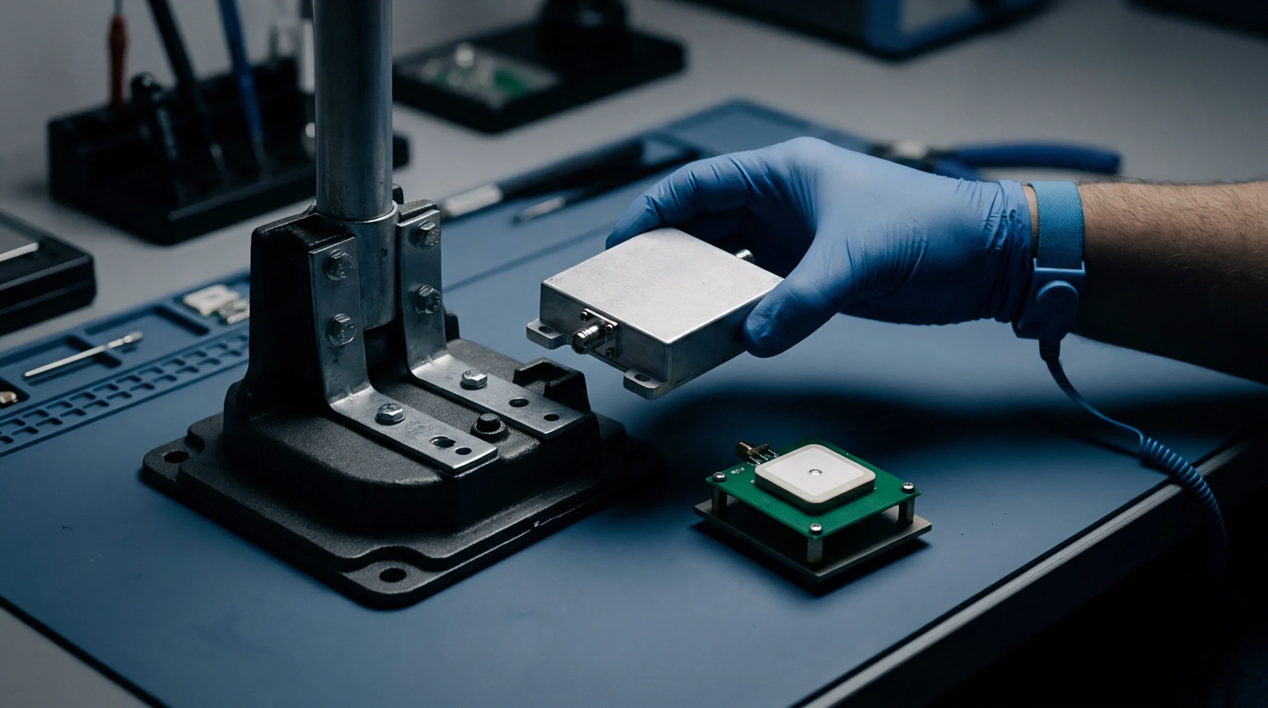
Board-to-board transitions rely on compression mount connectors or micro-coaxial assemblies to bridge discrete circuit boards without significant phase distortion. Solder joint geometry between radio frequency integrated circuits and the circuit board requires precise solder volume control, as excessive solder fillets introduce inductive discontinuities. Wire bonds create severe parasitic inductance at these wavelengths, requiring ribbon bonding or flip-chip interconnect configurations.
Gaskets fabricated from conductive elastomers seal mating metal housings, blocking cavity resonance effects around the physical transmission boundary.
Factory Qualification
Network analysis up to one hundred and ten gigahertz using ground-signal-ground microprobes validates insertion loss, return loss and group delay parameters on integrated test coupons. Time-domain reflectometry inspections confirm that localized impedance variations remain within five percent of nominal system targets. Connectors and joints undergo mechanical vibration and thermal cycling tests according to MIL-STD-883 Method 2002 to expose crack generation before factory sign-off.
Final acceptance requires automated test equipment to record flat passband performance and low return loss across operational millimeter-wave bandwidths.