Meaning
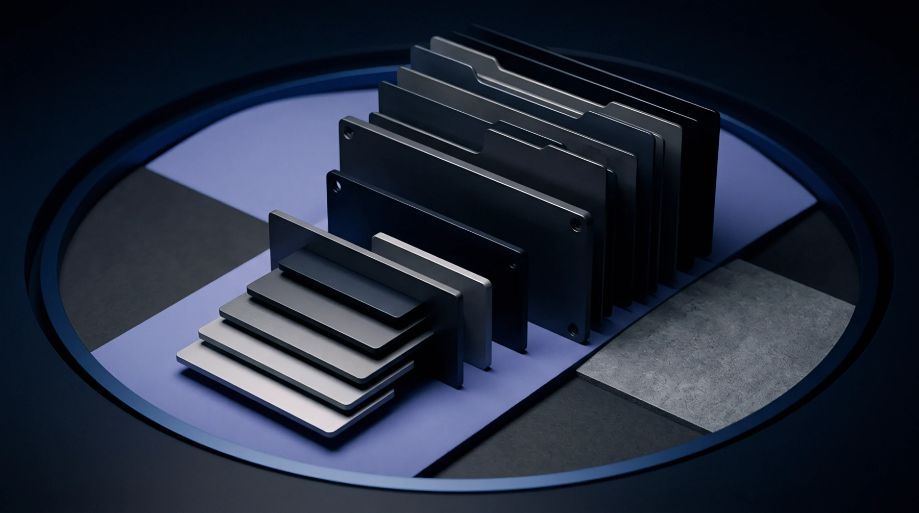
Layered arrangement of conductive copper foils and dielectric insulating substrates defines the physical architecture of a printed circuit board stackup. Engineers calculate signal integrity and impedance requirements to determine the specific sequence of these materials within the assembly.
Mechanical Constraint
Thermal expansion characteristics dictate the selection of materials to prevent warping or delamination during high heat cycles. Symmetric distribution of copper weights around the central core helps maintain structural balance during the lamination phase. Manufacturers monitor these material properties to ensure the finished board maintains its integrity throughout the reflow soldering process.
Electrical Performance
Precise spacing between conductive layers manages the crosstalk between high speed data lines that pass through the board. Electromagnetic compatibility standards depend on the grounding planes providing a return path for current. Designers adjust the thickness of prepreg layers to achieve the target impedance values required for reliable signal transmission.
Assembly Verification
Quality inspectors confirm the finished dimensions and layer registration against the original build documentation before the board moves to the component mounting stage. Cross section analysis reveals the internal geometry and material consistency of the laminate. Internal voids or misaligned vias indicate potential failure points that disqualify the unit from final production.