Meaning
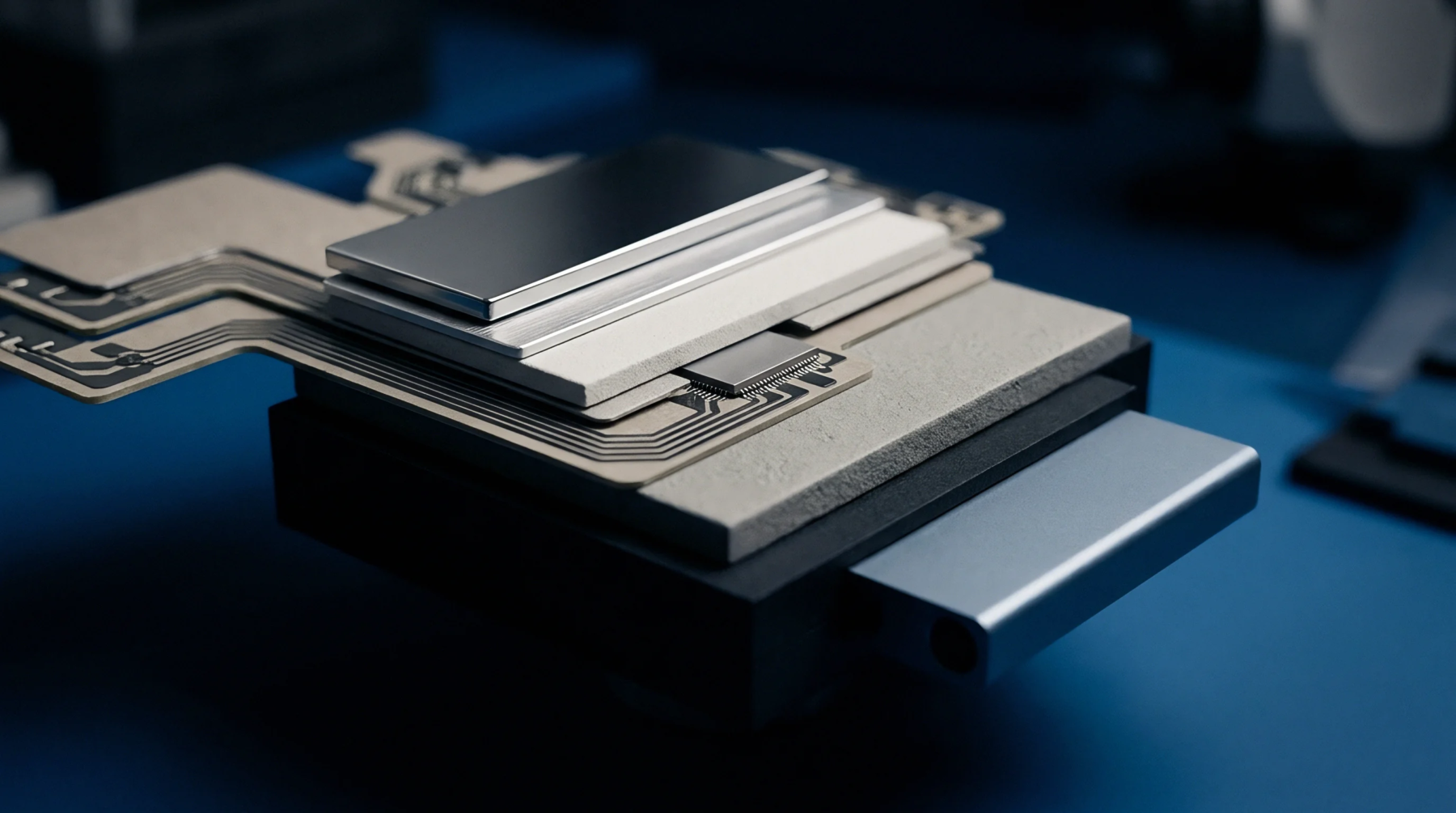
Package-level physical barriers isolate sensitive high-frequency transceiver circuits from external electromagnetic interference by enclosing miniature semiconductor substrates in conductive, grounded materials. Advanced microelectronic fabrication processes utilize system-in-package rf shielding to contain internal radio frequency radiation and block external noise inside space-constrained product enclosures. Conductive enclosures encapsulate complete multi-chip modules using selective trench isolation, conformal conductive coating techniques, or micro-machined internal metal lids mounted directly on the package.
The boundary applies to the microelectronic module assembly, terminating where external chassis shield cans and board-level shielding frames provide broader system isolation.
Coating Metallurgy
Microelectronics manufacturers apply thin conductive coatings directly across the exterior surfaces of molded epoxy resin packages using advanced physical deposition methods. PVD sputtering systems deposit precise multi-tier metal coatings, starting with an adhesive titanium base layer, continuing with a conductive copper or aluminum core, and concluding with a protective anti-corrosion layer like stainless steel. These ultra-thin deposited metal layers, typically three to five micrometers thick, provide effective electromagnetic attenuation without adding significant weight or thickness to the component.
The conductive coating connects to ground planes through exposed substrate perimeter solder points, providing a low-impedance path to dissipate unwanted RF energy. Laser etching techniques cut narrow boundary lines into the surface metal, preventing the conductive shield from shorting peripheral surface-mount component contacts.
Layout Decoupling
Integrating high-density radio modules alongside baseband processors requires careful printed circuit board layouts to maintain clean ground references. Module designers place dense arrays of grounded micro-vias around the package perimeter, creating an internal Faraday cage that blocks noise transmission through the substrate. High-frequency digital lines running underneath the component must not route adjacent to sensitive RF inputs, as substrate coupling can bypass package shielding.
Decoupling capacitors must sit as close as possible to package power pins, minimizing loop inductances that can radiate into internal antenna networks. Ground traces require broad copper pours that connect to main board internal planes through low-impedance paths, minimizing common-mode voltages during cellular bursts.
Verification Protocol
Production validation requires rigorous testing to confirm the mechanical durability, electrical continuity, and RF isolation of the package-level metal barrier. Automated test equipment measures surface resistance across the molded component face to verify uniform metal thickness and confirm solid electrical contact with package ground pins. Environmental stress chambers expose parts to thermal cycling from negative forty to positive eighty-five degrees Celsius, confirming that differing thermal expansion rates do not cause the metal coating to flake or peel.
Laboratory technicians use near-field sniffing probes in anechoic chambers to measure radiated emissions from the module, verifying that high-frequency noise drops by at least thirty decibels across target bands. The integration signoff document requires cross-sectional electron microscope imagery showing consistent, void-free metal coverage across package corners before approving the component for volume manufacturing.