Auditing Technical Documentation Completeness during Dual Source Manufacturing Transfer Package Bring-Up
Auditing transfer packages demands verifying native CAD files, bit-for-bit firmware build parity, ATE jig calibration logs, and ECN histories before tooling.


Anatomy
Auditing technical documentation for a dual-source manufacturing transfer means checking six core engineering deliverables for physical and functional parity before secondary tooling begins. A complete package gives the receiving facility the exact assets used at the primary site, removing ambiguity during setup. Discrepancies between what a contract design house exports and what an SMT line actually consumes cause immediate bring-up delays.
Rebuilding a printed circuit board assembly (PCBA) from truncated Gerber exports or compiled binary blobs wastes engineering hours reverse-engineering routing and firmware behavior. The audit starts by comparing the documentation archive against physical golden units taken straight from the primary factory line.
The primary baseline asset is the native computer-aided design (CAD) archive. Generating production tooling directly from raw Gerber data strips out netlist intelligence, component library shapes, and parametric layer stack-up definitions. Receiving sites need native format files such as Altium.PcbDoc and.PrjPcb , Cadence Allegro.brd , or KiCad.kicad_pcb formats along with associated schematic databases.
Native schematics preserve component parameter tables, differential pair rules, net class definitions, and internal design notes that flat PDF or Gerber renderings lose. Without these databases, secondary process engineers cannot run automated design-rule checks (DRC) or adapt land patterns to their specific SMT placement machine tolerances. Missing native files usually signal incomplete handoffs.
Firmware deliverables carry just as much operational risk when handoffs are incomplete. Secondary bring-up lines are often given final production hexadecimal or binary firmware files without the compiler toolchains, linker scripts, or configuration source trees behind them. A thorough audit looks for a fully reproducible build environment: version-locked C/C++ source code repositories, board support packages (BSP), chip vendor software development kits (SDK), compiler toolchain binaries, linker script.ld files, and automated build scripts.
If the secondary factory cannot compile the target source code to produce a bit-for-bit identical binary CRC-32 checksum, the firmware package fails the audit.
A documentation transfer package that relies on exported CAD files rather than native source archives forces the second factory to reverse-engineer board geometry.

Transfer Dossier Structure and Component Classifications
Organizing a transfer dossier into standardized data vaults prevents version drift across plants. Hardware transfer packages break down into distinct buckets: bare board fabrication data, SMT assembly archives, programmable device binaries, automated test equipment (ATE) fixtures, and mechanical engineering drawings. Each bucket should follow a strict file naming convention tied directly to its engineering change notice (ECN) state.
The bare board vault holds fabrication drawings, stack-up drill tables, and IPC-2581 or Gerber X2 files. The assembly vault contains pick-and-place centroid files, solder paste stencil artwork, bill of materials (BOM) database files, and high-resolution optical inspection reference images.
Component classification records in the bill of materials need to go beyond single-source manufacturer part numbers. Dual-sourcing breaks down quickly when a secondary factory hits long lead times on passives because alternate vendor specifications were omitted. A complete BOM maps internal part numbers (IPN) to at least two qualified manufacturer part numbers (MPN), explicit component package footprints per IPC-7351 guidelines, dielectric ratings for capacitors, temperature coefficients, and tolerance classifications.
For high-frequency radio frequency (RF) circuits, passive component specifications must also define equivalent series resistance (ESR) and self-resonant frequency (SRF) thresholds. Leaving these out leads purchasing teams to substitute passives that look equivalent on paper but degrade RF performance.
Baseline Deliverables for Dual-Factory Replication
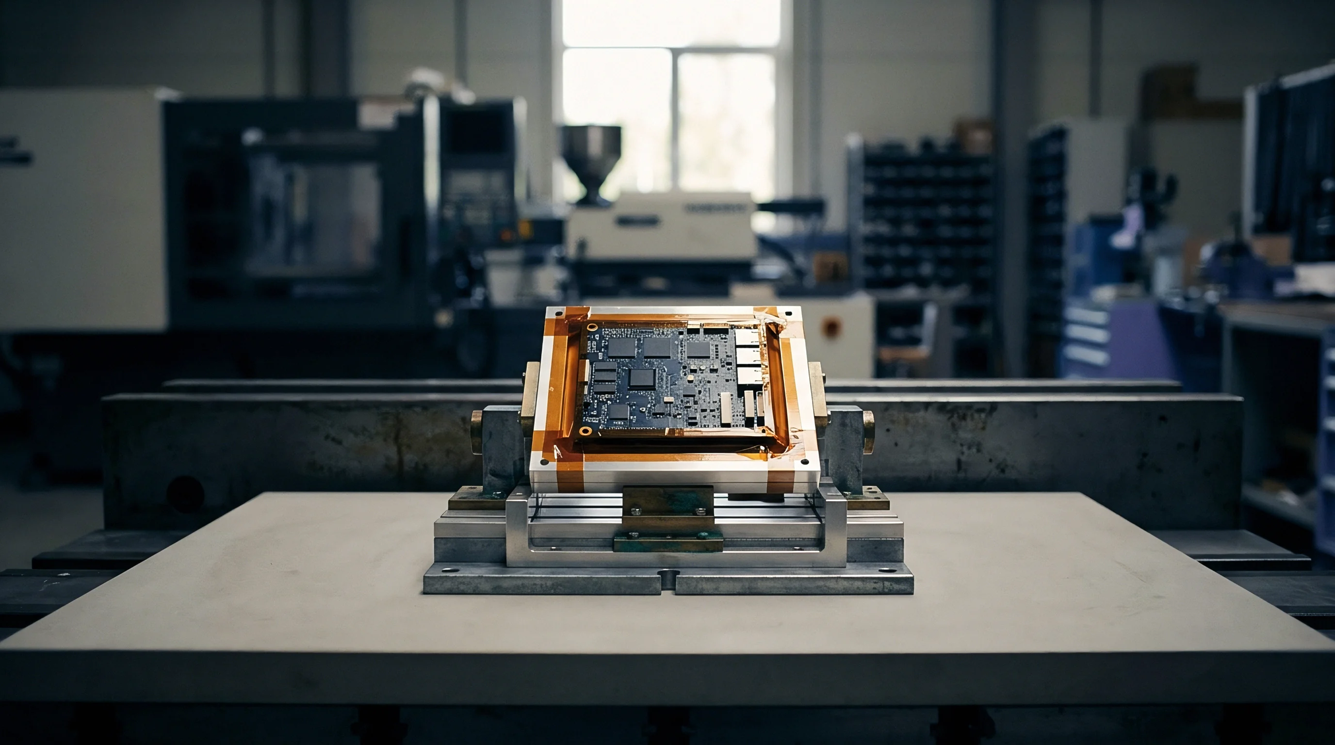
Validating mechanical tooling drawings is the final component of dossier auditing. Transfer packages must include native 3D STEP models of the populated board assembly, final enclosure assemblies, heat sink interface materials, and custom interconnect hardware. Dimensioned 2D engineering drawings in DXF or DWG formats need to specify critical tolerances, material finish grades, flame retardancy ratings under UL 94-V0, and fastener torque limits.
Without parametric 3D models, mechanical engineers at the receiving plant cannot verify spatial clearances inside injection-molded enclosures, which causes mechanical binding or thermal interface compression issues during box-build integration.
Automated test equipment coverage documentation sets the boundary for manufacturing accountability. The transfer package has to include complete schematics for test interface circuit boards, bed-of-nails Pogo pin wiring maps, test executive software source code, and primary-site calibration logs. A secondary factory cannot validate yield if its test fixtures execute different test scripts or use looser pass-fail thresholds than the original plant.
The audit verifies that every functional test step, test point coordinate, and power supply load condition matches the primary site specification down to the millivolt and milliampere.
| Artifact Category | Native Source Format | Functional Verification Method | Primary Defect Flag |
|---|---|---|---|
| CAD Schematic and Layout | Altium.PcbDoc , Cadence.brd | Native DRC execution, IPC-2581 netlist extraction | Exported Gerber files missing net intelligence |
| Firmware Source Tree | C/C++ git repository, ld scripts | Bit-for-bit binary compilation CRC matching | Binary-only hex files provided without source |
| Bare Board Fabrication | IPC-2581 Class 3, Gerber X2 | Controlled impedance solver, drill map audit | Flat Gerber files missing stack-up dielectric data |
| Bill of Materials | SQL/Excel database with IPN/MPN | Automated lifecycle and cross-reference audit | Single-source MPN without electrical tolerances |
| ATE Test System | Python/LabVIEW source, Pogo maps | Golden unit yield loop and limits audit | Compiled test executables without source code |
| Mechanical Assemblies | 3D STEP, 2D DXF with tolerances | 3D CAD clearance and thermal stack-up simulation | 2D flat PDF drawings lacking geometric tolerance |
Providing flat Gerber outputs and pre-compiled production binaries protects intellectual property and satisfies transfer agreements on paper, but initial runs fail quickly when core design intent remains locked inside unexported native databases.


Stack
Board layer construction dictates signal integrity, thermal dissipation, and mechanical warpage during SMT reflow. Primary sites build yield histories around specific substrate materials, copper foils, and prepreg glass styles. When secondary fabricators try to reproduce a high-density interconnect (HDI) printed circuit board without complete stack-up specifications, electrical performance shifts right away.
The secondary shop might select an alternative FR-4 laminate with the same nominal thickness but different dielectric constant (Dk) and dissipation factor (Df) metrics, which ruins impedance matching across high-speed digital buses and RF microstrip traces.
Transferring artwork through flat Gerber files strips essential layer stack-up parameters from the fabrication package. Standard Gerber RS-274X files describe only two-dimensional copper geometry, aperture shapes, and drill hole locations. They carry no embedded data regarding laminate Dk at operating frequencies, copper foil roughness profiles, prepreg resin content ratios, or target impedance specifications.
Secondary fabricators receiving plain Gerber files end up guessing dielectric spacing to hit overall board thickness requirements.
The IPC-2581 format solves this problem by encapsulating physical layout, netlist connectivity, layer stack-up definitions, material properties, and component assembly data inside a single XML schema. Auditing the fabrication package means confirming the presence of IPC-2581 Class 3 XML files or detailed, fully dimensioned fabrication drawings. These drawings must specify exact laminate materials, such as Isola FR408HR or Rogers RO4350B, finished copper weights for internal and external layers, via plating thickness, and solder mask dielectric properties.
Failure to stipulate IPC-2581 Class 3 XML outputs in the design transfer agreement leaves dielectric layer tolerances unconstrained during secondary factory bring-up.

CAD Geometry and Physical Layer Validation
Physical trace geometries on the bare board must match the impedance modeling from initial development. High-speed signals such as PCIe Gen 4, USB 3.2, and 50-ohm RF antenna feeds demand tight geometric control. A comprehensive audit checks that trace width, trace spacing, and copper ground plane clearances match native layout files precisely, verifying that single-ended traces fall within target tolerances ~ typically 50 ohms +/- 10% ~ and differential pairs maintain specified differential impedance, such as 90 ohms or 100 ohms +/- 10%.
Fabrication notes should specify acceptable manufacturing tolerances per IPC-6012 Class 2 or Class 3 standards. Board shops routinely adjust trace widths on photoplotting tooling to compensate for chemical etching undercut. Without explicit instructions covering target finished trace widths versus starting copper foil weights, secondary fabricators can easily over-etch or under-etch traces, altering system impedance.
Thermal relief pad geometries, teardrops at via junctions, and microvia aspect ratios must also be audited against native design rules to preserve mechanical reliability under thermal cycling.

Which File Format Controls the Fabrication Stack-Up?
Deciding whether IPC-2581 XML archives or traditional Gerber RS-274X datasets govern bare board manufacturing rights clears up tooling conflicts before fabrication starts. Standardizing on IPC-2581 XML eliminates manual stack-up reconstruction by secondary fabricators. Gerber RS-274X files rely on separate text-based drill tables, fabrication drawings, and stack-up spreadsheets, a multi-file setup that regularly introduces error when CAM operators manually transcribe layer orders and dielectric thicknesses into plant-specific software.
When dual-sourcing high-frequency or high-density boards, IPC-2581 files carry explicit material callouts linked directly to CAD net names. The secondary factory’s CAM system reads dielectric constant values straight from the file, enabling automated impedance checks against local production capabilities. If the primary package only contains Gerber RS-274X data, the audit team needs a signed fabrication drawing with a complete impedance control table detailing layer numbers, signal trace widths, reference plane layers, dielectric spacing, target impedance values, and acceptable tolerance windows.
- Dielectric mismatch occurs when secondary board shops substitute lower-cost laminates with higher dissipation factors, attenuating high-frequency signals and causing data packet drops.
- Unresolved footprint substitutions lead to pad-to-lead misalignments during SMT placement, causing tombstoning or solder bridging across fine-pitch QFN and BGA components.
- Missing copper balance rules cause asymmetrical copper distribution across internal layers, inducing board twist and bow that exceeds IPC-A-600 flat-ness limits during reflow.
- Omitted testpoint coordinates prevent ATE bed-of-nails pin alignment, breaking automated in-circuit testing and forcing manual bench debugging on secondary production boards.
Secondary fabricators receiving incomplete stack-up documentation inevitably default to local substrate materials and dielectric spacings to meet nominal board thickness targets. Sending unconstrained copper artwork without embedded IPC-2581 material specifications turns board fabrication into a high-stakes guessing game.

Discrepancy
Hardware fabrication accuracy guarantees nothing if secondary plants program target devices using non-reproducible firmware packages or run validation on uncalibrated test rigs. Firmware builds and automated test equipment (ATE) setups account for most silent failures in dual-source transfers. A secondary factory can assemble a physically flawless PCBA, yet end up with zero yield because of minor toolchain differences or incorrect test box attenuation factors.
Auditing these packages requires strict validation of compilation inputs and test hardware configurations.
Firmware source archives must include explicit dependencies down to exact compiler binary release numbers, build system flags, and target microcontroller fuse settings. If the primary site compiles source code using GNU Arm Embedded Toolchain version 10.3-2021.10 with specific optimization options like -O2 and -flto , the secondary factory must mirror that environment exactly. Compiling the same C/C++ codebase with a different GCC release or altered optimization levels shifts memory footprint allocations, interrupt execution timing, and peripheral register initialization.
The transfer audit verifies reproducible build setups, ideally packaged inside container environments like Docker. A containerized toolchain encapsulates operating system dependencies, build tools, compiler releases, and image generation scripts. Compiling firmware inside a verified container ensures both plants output identical binary executables with matching CRC-32 or SHA-256 hashes.
Any package failing binary checksum verification indicates hidden environment differences that will surface later as intermittent field defects or timing failures.
A deviation of 0.8 dB in test jig fixture attenuation across 5.8 GHz frequencies invalidates pass-fail yield parity between primary and secondary production lines.

Firmware Compilation Environments and Binary Parity
Validating programmable device artifacts requires inspecting every step in the programming pipeline. Microcontrollers, Field Programmable Gate Arrays (FPGA), and wireless system-on-chips (SoC) rely on complex flash memory layouts. The documentation package must detail primary bootloader memory maps, application code start addresses, persistent configuration sectors, and security keys.
Fuse settings, option bytes, and security configuration scripts must be explicitly documented alongside production hex files.
FPGA bitstreams require complete synthesis project files, constraints files (.sdc or.xdc ), and IP core configuration states. Providing a final bitstream binary without underlying HDL source files (VHDL or Verilog) prevents secondary engineers from debugging timing closure issues or patching minor bugs during bring-up. The audit enforces full access to native FPGA project source trees so secondary teams can perform synthesis, place-and-route, and timing verification locally.

Automated Test Equipment Fixtures and Calibration Audit
Test fixture discrepancies account for most false failure rates logged during secondary plant bring-up. An ATE setup consists of custom physical test jigs, bed-of-nails Pogo pin plates, signal conditioning boards, power supplies, spectrum analyzers, and test executive software. If the primary factory relies on custom Python test scripts executing on specific driver versions, the secondary site must run identical software builds.
Auditing the ATE deliverable mandates a thorough review of test scripts, measurement algorithms, and pass-fail limit files.
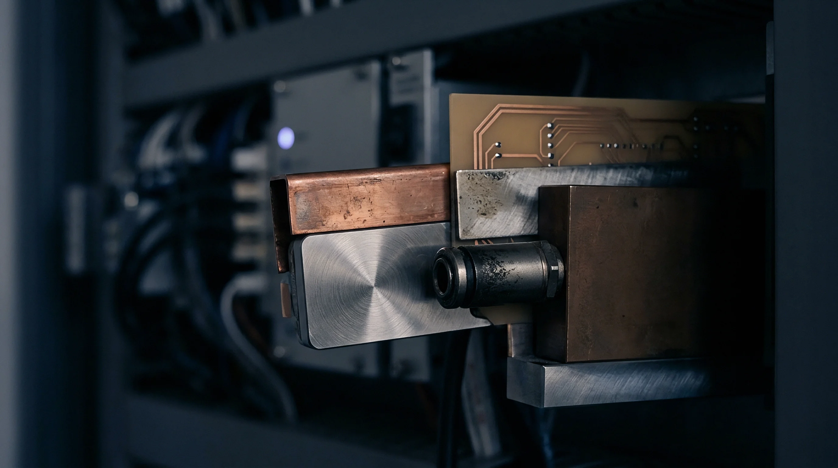
Physical fixture calibration logs must accompany every ATE hardware transfer. Bed-of-nails test jigs experience mechanical pin wear, spring relaxation, and contact surface contamination over long production runs. Pogo pin contact resistance must remain below 50 milliohms per pin to prevent voltage drop measurement errors during functional test execution.
RF testing fixtures demand precise path loss measurement logs, since coaxial cables, RF switches, and shielding box enclosures introduce signal attenuation that must be offset within test software parameters.
| Evaluation Metric | Primary Site Baseline | Secondary Site Target | Maximum Allowed Variance | Audit Remediation Action |
|---|---|---|---|---|
| Firmware Binary Hash | CRC-32 / SHA-256 Match | 100% Binary Identical | 0 Bit Variance | Rebuild inside container |
| ATE Pogo Pin Resistance | Less than 20 mOhm | Less than 50 mOhm | +30 mOhm Drift | Clean or replace Pogo pins |
| RF Path Loss Attenuation | -1.2 dB offset at 2.4 GHz | -1.2 dB offset at 2.4 GHz | +/- 0.2 dB Offset | Recalibrate RF cable path |
| Functional Power Limits | 3.3V Line @ 150mA +/-5% | 3.3V Line @ 150mA +/-5% | 0mA Delta Limit | Verify PSU load sensing lines |
| FPGA Timing Margin | +1.8 ns Setup Slack | +1.8 ns Setup Slack | 0.0 ns Slack Loss | Re-run timing constraints check |
Tracking firmware compilation and ATE calibration records across multiple transfers reveals where systems begin to diverge. Deploying unverified firmware compiler configurations or uncalibrated functional test jigs to a secondary manufacturing plant leads to elevated scrap rates, invalid warranty failures, and prolonged production line downtime.


Vault
Bill of materials records and engineering change notice archives form the commercial core of hardware manufacturing documentation. A bare board drawing and firmware repository cannot build a physical product without a fully qualified, multi-tier BOM linked to verified supply chains. Dual-sourcing initiatives break down when secondary purchasing teams attempt to procure components using incomplete internal part numbers or unverified alternate vendor cross-references.
Managing BOM audits requires checking part lifecycle status, physical component packaging, and historical engineering changes.
A production BOM must map internal part numbers to complete manufacturer part numbers with zero missing suffixes. Suffixes in electronic component part numbers specify critical parameters like pin plating materials, tape-and-reel packaging formats, operating temperature ranges, and internal silicon revisions. For example, a microchip part number missing its final suffix code can lead to ordering bulk tube-packaged ICs instead of tape-and-reel formats compatible with high-speed automated SMT pick-and-place feeders.
The BOM audit confirms that every IPN maps to active, fully specified MPNs from established distribution networks.
Auditing alternate vendor lists (AVL) prevents unexpected stockouts during secondary bring-up. Passive components like ceramic capacitors and chip resistors should feature multiple approved vendors per IPN. For critical active components such as voltage regulators, microcontrollers, and operational amplifiers, alternate parts must undergo rigorous electrical characterization before joining the approved vendor list.
Substituting an operational amplifier with a secondary part that matches gain bandwidth product can still introduce instability if the alternate device has different phase margin or input bias current profiles.

Bill of Materials Auditing and Approved Vendor Lists
Detailed component characterization data forms the basis of BOM compliance verification. Inductors present subtle dual-sourcing challenges: substituting a power inductor with a second-source component matching nominal inductance and continuous current ratings can still introduce switching regulator instability if saturation current (Isat) or DC resistance (DCR) ratings differ. The documentation package must include explicit engineering specifications for every custom magnetics component, high-precision resistor, and low-ESR electrolytic capacitor, which the audit validates against thermal and electrical operating envelopes.
Component lifecycle auditing identifies obsolete or near-end-of-life (EOL) components before manufacturing rights are transferred. A transfer package containing EOL parts forces secondary plants into expensive component re-qualification cycles immediately after bring-up. The audit checks every MPN against component lifecycle databases, flagging Last Time Buy (LTB) notices, EOL announcements, and Engineering Change Notices from semiconductor manufacturers.

Engineering Change Notice Reconstruction and Traceability
Tracking historical design changes across primary factory production runs ensures the secondary site builds the current product revision. Engineering Change Notices record hardware modifications, PCB trace cuts, jump-wire additions, component value swaps, and firmware updates implemented during initial manufacturing setup. Primary factories often make minor redwire modifications or passive component tweaks on the shop floor to boost yield without updating the central CAD schematic or BOM baseline immediately.
Reconstructing the complete ECN lineage from Revision A to the current production revision reveals hidden shop-floor adjustments. The transfer audit cross-checks physical golden units pulled from the primary line against the delivered CAD schematics and assembly drawings. If inspection of primary golden units reveals 0201 bypass capacitors soldered directly across IC pins or hand-soldered modification wires missing from CAD source files, the transfer package fails the audit.
The primary plant must update all native schematics, Gerber archives, and BOM records to reflect the true production state.
- Download primary factory raw production logs and compare current component reel part numbers directly against delivered BOM database entries to surface unrecorded shop-floor component substitutions.
- Match physical reel part numbers against approved vendor list records to isolate unauthorized component substitutions implemented to solve local component shortages.
- Run differential netlist comparison scripts between native schematic files and CAD layout netlists to verify that late schematic updates propagated to physical layout copper structures.
- Verify thermal profile data and reflow furnace settings used by the primary plant to establish baseline thermal limits for secondary manufacturing process setup.
Section 4.2 of IPC-9210 binds the primary vendor to furnish complete ECN history ledgers before secondary line tooling starts. Failing to enforce complete ECN tracking results in secondary plants building obsolete design revisions that reproduce old operational bugs.


Replication
First article inspection and initial bring-up runs at secondary plants provide the final empirical test of transfer package completeness. Theoretical audits of CAD files, BOM databases, and firmware repositories cannot catch every subtle manufacturing dependency. Executing a controlled 500-unit pilot production run at the secondary site reveals process gaps, tooling mismatches, and document omissions under actual factory conditions.
Achieving yield parity between sites proves that the secondary facility possesses complete design knowledge.
Missing deliverables correlate directly with first-article yield drops, with 68% of initial secondary yield failures tracing to unmapped functional test thresholds, incomplete component specifications, or unrecorded solder reflow thermal profiles. Achieving first pass yield (FPY) parity requires executing identical test procedures and subjecting first-article units to statistical process control (SPC) analysis, measuring Cpk process capability indices across critical electrical parameters.
First Pass Yield calculation sums all units passing functional testing on the first attempt without rework, divided by total units tested:
FPY = left( fracNpassNtotal right) × 100
Process Capability Index (Cpk) evaluates how closely secondary factory performance matches primary engineering specification limits (USL = Upper Specification Limit, LSL = Lower Specification Limit, μ = sample mean, σ = sample standard deviation):
Cpk = minleft( fracUSL – μ3σ, fracμ – LSL3σ right)
A dual-source bring-up achieves statistical parity when the secondary facility demonstrates Cpk ge 1.33 across key performance parameters, matching primary site baselines.
First pass yield discrepancies between manufacturing sites trace to unmapped test jig contact resistance variations rather than component silicon tolerances.
Bring-Up Bench Execution and Yield Parity Metrics
Statistical validation requires subjecting both primary and secondary first-article batches to identical measurement protocols. Key parameters include RF transmitter output power, receiver sensitivity, power supply rail ripple under transient loading, and current consumption during low-power sleep modes. If primary factory units exhibit RF transmit power of +20 dBm +/- 0.5 dB with a Cpk of 1.45, but secondary factory units show +20 dBm +/- 1.2 dB with a Cpk of 0.88, the secondary process is out of control.
Thermal reflow profiling is another critical variable during first-article replication. Secondary factories utilize different SMT reflow ovens with distinct heating zones, convection rates, and belt speeds. The transfer package must supply primary furnace temperature profiles, solder paste chemistry specs (e.g.
SAC305 lead-free alloy), and maximum allowable thermal ramp rates. Secondary process engineers need to instrument test boards with thermocouples to adjust local reflow zone temperatures, preventing thermal shock, voiding, or incomplete solder wetting on large thermal ground pads.

Root-Cause Analysis of Dual-Source First Article Discrepancies
Isolating the root cause of bring-up discrepancies requires systematic diagnostic protocols. When secondary first-article units show elevated failure rates during functional testing, diagnostic engineering follows a structured isolation sequence: swapping golden firmware binaries, isolating test jig hardware, and running cross-factory component swaps. Swapping a primary-built board into a secondary test fixture immediately reveals whether the test fixture or the board itself holds the defect.
Solder joint voiding beneath bottom-termination components like QFNs and BGAs is a frequent cause of intermittent thermal and ground impedance failures. IPC-A-610 Class 3 standards require total solder voiding beneath thermal pads to stay under 25%, with individual voids taking up less than 9% of the total pad area. X-ray inspection of first-article units from both sites confirms whether stencil thickness, aperture cross-hatching design, and reflow profile settings match primary baseline quality levels.
| Production Quality Metric | Primary Factory Baseline | Secondary Factory Initial | Secondary Post-Audit | Parity Acceptance Limit |
|---|---|---|---|---|
| First Pass Yield (FPY) | 98.4% | 89.1% | 98.1% | Within 0.5% of Primary |
| Cpk (RF Output Power) | 1.48 | 0.92 | 1.42 | Cpk ge 1.33 Minimum |
| QFN Thermal Pad Voiding | 14.2% Area | 28.6% Area | 15.1% Area | Less than 25% Total (IPC Class 3) |
| Sleep Current Consumption | 12.4 uA +/- 0.8 uA | 18.9 uA +/- 3.4 uA | 12.6 uA +/- 0.9 uA | Within +/- 1.0 uA of Baseline |
| Solder Bridging Defect Rate | 45 PPM | 380 PPM | 52 PPM | Less than 60 PPM Target |
Engineers continue to debate whether thermal pad voiding tolerances should be tightened below 15 percent for dual-sourced high-frequency power amplifiers operating in high-vibration industrial environments.


Arbitration
Assigning non-recurring engineering (NRE) costs and establishing commercial liability boundaries determines financial accountability when design transfer packages prove incomplete. Contract engineering design houses and turnkey manufacturing partners often quote baseline transfer fees that cover only flat Gerber exports and binary hex drops. When secondary bring-up runs stall due to missing native CAD files, uncalibrated test scripts, or incomplete BOM specifications, disputes arise over who pays for corrective engineering hours.
Structuring transfer contracts with explicit documentation acceptance criteria protects secondary purchasers from unexpected cost overruns.
A well-drafted manufacturing transfer agreement establishes a clear division of labor quantified in engineering hours. The contract specifies exact deliverables required for package sign-off, detailing file formats, firmware compile checks, and test fixture delivery. If the primary supplier fails to provide reproducible firmware build scripts or native IPC-2581 datasets, the agreement mandates that the supplier perform remediation work under capped NRE budgets or forfeit transfer milestone payments.
Escrow accounts provide commercial protection for critical intellectual property during turnkey or white-label manufacturing transfers. When a primary supplier refuses to release native schematic CAD source files over IP exposure concerns, the agreement can mandate placing native source code, PCB design files, and ATE test scripts into a secure third-party escrow account. If the primary supplier experiences insolvency, fails to meet defined unit delivery schedules, or unilaterally terminates supply agreements, escrow release conditions trigger, granting the buyer full access to complete technical documentation.

Scope Boundaries and Engineering Hour Allocations
Quantifying engineering effort during transfer package bring-up prevents invoice scope creep. Bring-up projects require dedicated allocations across distinct engineering disciplines: 160 hours for bare board CAM setup and stack-up validation, 80 hours for ATE script translation and test jig calibration, 60 hours for BOM lifecycle verification, and 40 hours for SMT reflow profile optimization. Defining these scope limits in the statement of work establishes a clear baseline for assessing extra NRE charges caused by incomplete vendor documentation.
Commercial contracts must define liability parameters for line downtime and scrap materials generated during secondary bring-up runs. If an incomplete documentation package leads the secondary plant to assemble 1,000 PCBA units with incorrect passive component values, the primary design owner or supplier responsible for documentation sign-off must absorb material scrap and rework costs. Incorporating clear technical completeness checklists directly into commercial purchase agreements turns vague documentation promises into enforceable engineering obligations.

Commercial Liability and Intellectual Property Transfer Verification
Final commercial sign-off requires executing an intellectual property transfer audit alongside technical validation. The buyer must confirm that all delivered design schematics, PCB layout files, test scripts, and firmware code repositories carry clear ownership titles free of encumbrances or third-party license violations. Open-source software licenses inside transferred firmware packages demand strict auditing: incorporating GNU General Public License (GPL) code into proprietary device firmware without compliance documentation exposes the buyer to copyright infringement claims and forced code disclosure.
The technical documentation audit ends when the secondary manufacturing facility completes a qualified pilot production run, achieves target First Pass Yield, and verifies bit-for-bit firmware compilation parity. Signing the final transfer acceptance certificate releases escrow funds, transfers tooling ownership rights, and authorizes volume production ramp-up at the secondary facility.
- Source file escrow retention protects access to native CAD files and firmware source trees if primary suppliers default on volume manufacturing supply commitments.
- Non-recurring engineering capped billing restricts engineering hour expenses incurred while resolving documentation errors during secondary factory setup.
- Acceptance testing milestone sign-offs shift commercial liability from buyer to supplier upon verification of First Pass Yield parity across dual production lines.
- Component lifecycle warranty clauses enforce supplier financial liability for component redesign expenses if transferred BOMs contain unnotified end-of-life parts.
Contractual transfer agreements that tie final NRE milestone payouts directly to empirical first-article yield parity resolve commercial disputes before secondary bring-up starts. The secondary factory assumes full production responsibility once all native source files, calibration scripts, and verification metrics pass final cross-audit sign-off.