Implementing Multi-Wavelength Dispersion in Optical Metrology Tooling
Implement multi-wavelength dispersion tooling by selecting an integration tier that matches production volume against optical design transfer ownership rights.

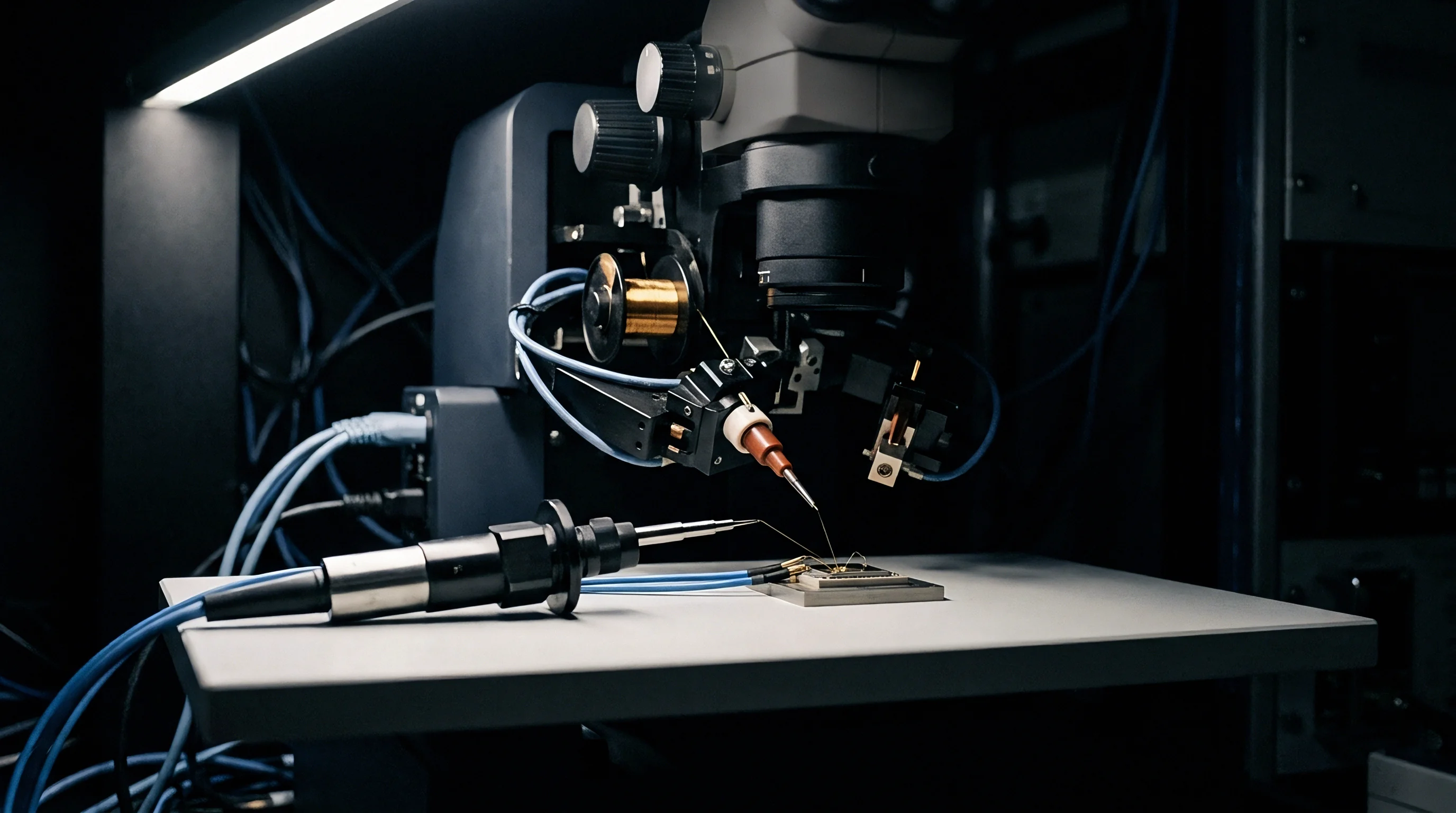
Slit
Resolving thin-film phase anomalies across broad spectral regimes requires careful chromatic dispersion compensation. In advanced semiconductor nodes, spectroscopic reflectometers and ellipsometers run into severe optical path variations when broadband illumination spans 190 nanometers through 1000 nanometers. Across that deep-UV to near-infrared window, entrance slit geometry governs both optical throughput and resolving power.
Narrowing the slit sharpens spectral resolution, but it chokes off photon flux right at the ultraviolet wavelengths where deuterium arc lamps already produce minimal output.
When specifying turnkey optical sub-assemblies, designers choose between fixed-aperture slits and motorized variable designs. Fixed slits avoid mechanical backlash and stay spatially repeatable. A 25-micrometer etched air slit, for instance, holds 0.8 nanometers of optical resolution across a 1024-pixel linear charge-coupled device array.
Throughput collapses below 240 nanometers, however, tripling signal integration times on ultra-thin dielectric layers. Motorized slits can adjust entrance widths between 10 micrometers and 100 micrometers to match the active channel, but mechanical slit actuators bring hysteresis that chips away at photometric accuracy during extended measurement runs.
A dual-lamp optical metrology sub-assembly yields less than five picowatts per nanometer of usable spectral irradiance at 193 nanometers when configured with a fixed 25-micrometer entrance slit.
Beam-splitter choice dictates how those multi-wavelength channels split physically. To dodge glass absorption in the deep UV, metrology engines route light to separate spectrometer benches. The UV path relies on reflective off-axis parabolic mirrors to prevent chromatic aberration, while refractive doublets focus visible and near-infrared light onto secondary detector planes.
Every added optical surface, though, brings polarization-dependent phase shifts that compromise ellipsometric accuracy.

How Does Channel Splitting Impact Spectroscopic Accuracy?
Reflective dichroic splitters separate light into discrete detection bands. A long-pass dielectric separator set at 45 degrees will bounce wavelengths below 400 nanometers into a Czerny-Turner spectrometer bench and pass 400 nanometers to 1000 nanometers through to an extended-range silicon photodiode array. That dielectric boundary is thermally sensitive, shifting its edge by 0.05 nanometers per degree Celsius.
Without cooled optomechanics, the shifting spectral power distribution across detector pixels shows up as artificial film thickness variations during automated wafer runs.
Buying teams have to weigh the trade-offs between turnkey spectrometer engines and custom optical benches. A turnkey unit arrives sealed, with factory-potted optics, a fixed grating mount, proprietary digitizer boards, a binary driver library, and an acceptance sheet verifying the spectral range. If the tool builder cannot modify internal dispersion parameters, they are stuck with whatever line spread function the vendor tuned at the factory.
Drift in deep-ultraviolet fringe visibility often stems from spectrometer slit blooming rather than ambient process chamber vibration.
Drift
Thermal gradients across high-dispersion diffraction gratings translate immediately into wavelength registration errors. Holographic gratings mounted on aluminum kinematic plates expand at 23 parts per million per degree Celsius. A shift of just two degrees displaces peak line positions on a 2048-element linear photodiode array by 1.4 pixels, which the metrology engine misinterprets as an apparent change in film refractive index.
Wavelength stability is tracked against atomic emission lines. Low-pressure mercury-argon calibration lamps inject reference peaks at 253.65 nanometers, 435.83 nanometers, and 546.07 nanometers into the collection fiber. System calibration maps these emission lines against pixel coordinates, deriving dispersion coefficients through a third-order Chebyshev polynomial fit.
Any pixel registration drift that occurs between calibration cycles feeds directly into layer thickness calculation errors.
Baseline drift depends on how tightly detector temperature is controlled. Back-thinned charge-coupled devices chosen for UV quantum efficiency rely on thermoelectric coolers. Chilling the silicon array to minus ten degrees Celsius cuts thermal dark current down to ten electrons per pixel per second.
However, analog proportional-integral control loops can still couple to ambient temperature swings if exhaust from the heat sink is poorly shielded inside the metrology frame.
| Sub-Assembly Integration Level | Grating Substrate Material | Wavelength Drift (pm/K) | Dark Current Drift (e-/pix/s/K) | Recalibration Interval (Hours) |
|---|---|---|---|---|
| Turnkey Spectrometer Engine | Soda-Lime Glass | 18.4 | 4.2 | 2 |
| Semi-Custom Optical Bench | Fused Silica | 4.1 | 1.1 | 8 |
| Custom Aplanatic Monochromator | Zero-Expansion Glass-Ceramic | 0.3 | 0.2 | 72 |
Mounting stress easily distorts the optical plane. Over-torquing retaining rings warps concave reflective mirrors and introduces astigmatism. When the focal spot degrades, optical power spills outside the active pixel area, degrading signal-to-noise at the edges of the spectrum.
Kinematic mounts with three-point hardened steel ball interfaces isolate the optical cell from chassis twist. Machining mirror cells out of matched titanium alloys helps preserve focal distance across cleanroom thermal cycles.
Contamination also degrades dispersion linearity over time. Exposure to 193-nanometer photons cracks trace hydrocarbons in the optical path, leaving graphitic carbon on the grating rulings. A ten-nanometer carbon film cuts diffraction efficiency in the vacuum ultraviolet by 40 percent.
Compensating for lost UV throughput requires longer exposure times, which slows wafer throughput on the line.
A spectral shift of just half a detector pixel across the ultraviolet band leads the metrology engine to miscalculate dielectric gate oxide thicknesses by tenths of an angstrom.

Firmware
Embedded pipelines convert raw pixel arrays into calibrated spectra. FPGA firmware handles offset subtraction, gain equalization, and non-linearity correction at rates above two kilohertz. The digitized output then passes through a dispersion matrix before entering host inversion models.
Rounding errors in fixed-point DSP math can compress dynamic range, especially when raw pixel counts approach sensor saturation.
Dark current corrections must handle spatial non-uniformity across the sensor. The firmware maintains baseline values for each pixel across sixteen discrete thermal bins, subtracting the appropriate bin offset before flat-field normalization. If exposure timing is not locked to lamp power ripple, periodic modulation bleeds into the extracted dispersion curves.
Optical calibration data transfers remain legally governed by factory acceptance procedures that disqualify sub-assembly deliveries exhibiting uncompensated spectral non-linearity exceeding 0.05 percent across the primary detection band.
Wavelength calibration algorithms reconstruct continuous dispersion profiles from discrete pixel indices through polynomial expansion. The firmware calculates:
Wavelength equals C0 plus C1 times pixel index plus C2 times pixel index squared plus C3 times pixel index cubed.
Factory calibration flashes coefficients C0 through C3 into non-volatile memory. Replacing a detector array requires rewriting those coefficients on the sub-assembly itself. Many module vendors lock calibration access, requiring customers to return the entire spectrometer engine to the factory simply to swap a sensor.

When Do Firmware Interfaces Compromise Tool Integration?
Integration stalls when vendors supply pre-compiled binary drivers that fail to track Linux kernel updates. Metrology host machines running enterprise real-time environments need direct memory access to high-speed digitizers. Opaque driver libraries obscure register-level communications, making it difficult for software teams to synchronize spectrometer triggers with stage encoders.
Missing microsecond-level timing windows during handshakes introduces physical registration offsets on patterned wafers.
To avoid proprietary lock-in, tool teams have to negotiate explicit software deliverables into procurement contracts. Turnkey agreements keep firmware source code locked inside supplier repositories. Semi-custom contracts, by contrast, should mandate access to raw register maps, clean APIs, and bare-metal initialization routines.
Owning the low-level diagnostic layer lets engineers isolate pipeline defects without waiting on vendor support tickets.
- Raw register maps define memory addresses for hardware trigger control, pixel clock configuration, and analog front-end programmable gain settings.
- Firmware source repositories contain synthesizeable register-transfer-level hardware description code alongside embedded microcontroller firmware source trees.
- Hardware interface toolkits provide documented driver application programming interfaces compatible with standard host operating systems alongside reproducible build scripts.
Modifying clock generation circuits on the digitizer alters sensor integration duty cycles, invalidating factory non-linearity tables across every operational mode.
Handover
A thorough design transfer package provides the only real autonomy for a metrology integrator. Buying a turnkey spectrometer removes initial mechanical design work, but it creates long-term configuration vulnerabilities. Moving from prototype builds to volume production quickly exposes gaps in the drawing package.
Integrators need full solid models, optical fabrication specs, electronic schematics, and test bench runbooks before issuing volume purchase orders.
Optical drawings require tight tolerances to ensure tool-to-tool matching. Reflective mirrors typically demand surface figure accuracy down to one-twentieth of a helium-neon laser wavelength and micro-roughness below 0.5 nanometers root-mean-square. Coating callouts must specify spectral reflectance profiles, outgassing durability in cleanroom environments, and damage thresholds.
Leaving off scratch-dig tolerances per MIL-PRF-13830B risks receiving optics that scatter deep-UV energy, skewing the tool’s baseline reflectance.
Optical component drawings lacking surface figure tolerances below tenth-wave limits cause inter-tool film thickness discrepancies exceeding one percent across parallel cleanroom process tracks.
Electronics packages need to include raw PCB artworks alongside fully populated bill-of-materials databases. Sensor interface boards rely on low-noise transimpedance amplifiers that resolve sub-picoampere photocurrents. Documentation must call out critical passive ratings, dielectric stack-ups, and trace clearance rules.
Swapping an operational amplifier during supply shortages can alter analog bandwidth, adding phase lag to high-speed acquisitions.
Dual-sourcing depends on duplicate alignment and calibration fixtures. Integrators must replicate bring-up benches equipped with multi-axis interferometers, wavelength reference sources, and automated beam profilers. If the transfer package omits test software source code, second-source facilities cannot validate alignment, and production stalls when alternative assemblers cannot reproduce original factory acceptance tests.
- Optical fabrication dossiers detail substrate materials, mechanical boundary dimensions, coating performance envelopes, clear aperture definitions, and wavefront distortion test methodologies.
- Schematic capture databases supply editable native electronic design files, multi-layer printed circuit board layout archives, gerber output streams, and component pick-and-place coordinates.
- Alignment fixture blueprints detail optomechanical alignment benches, manual micrometer stages, kinematic adjustment protocols, and interferometer test targets.
- Acceptance testing procedures define spectral resolution verification routines, stray light assessment techniques, signal-to-noise ratio measurements, and thermal stability qualification periods.
Semi-custom contracts must establish boundaries around proprietary optomechanics and design records. The integrator typically negotiates full assignment for custom adapter plates, housing geometries, and harnesses, while the module supplier retains background IP on detector arrays and grating mastering methods. Defining these boundaries early prevents ownership disputes if the tool builder re-sources secondary assemblies.
Under Section 8.4 of standard design service agreements, ownership of all contract manufacturing deliverables transfers upon final invoice payment, extinguishing proprietary supplier claims to production test software.

Margin
Integrating an optical engine balances non-recurring engineering against recurring unit cost. Turnkey spectrometers demand little upfront capital but leave every shipped tool carrying a high bill-of-materials cost. Custom or semi-custom assemblies require heavy initial development spending but bring down volume piece costs, leaving OEMs to calculate breakeven horizons against projected cleanroom tool shipments.
Engineering scope governs upfront investment. Contracting an optical firm for a custom dispersion bench typically takes 800 to 1400 engineering hours: roughly 300 hours for optical optimization, 350 for optomechanics, 300 for firmware, and 250 for system integration and validation testing. At standard rates of 180 dollars per hour, non-recurring engineering reaches 216,000 dollars before manufacturing physical prototypes.
| Integration Model Scope | Initial NRE Cost (USD) | Prototype Tooling Cost (USD) | Unit Production Price (USD) | Total Programme Expenditure (USD) |
|---|---|---|---|---|
| Turnkey Standard Engine | 15,000 | 0 | 14,500 | 3,640,000 |
| Semi-Custom Modified Bench | 95,000 | 35,000 | 8,200 | 2,180,000 |
| Full Custom Bespoke System | 220,000 | 85,000 | 4,800 | 1,505,000 |
Lower unit costs in custom architectures come largely from stripping out unused features. Commercial turnkey units carry generic sheet-metal enclosures, multi-purpose interface boards, and display logic unnecessary in production wafer tools. Custom designs bypass those extras, piping raw sensor signals directly to the tool’s central backplane and eliminating separate enclosures, dedicated power supplies, and external cabling.
Custom engineering shifts component obsolescence entirely onto the tool builder. Commercial vendors absorb sensor redesigns, passive component end-of-life notices, and microcontroller transitions into their margins. With a custom optical engine, the tool builder must monitor the supply chain directly, often holding strategic buffer stock of critical image sensors and programmable logic devices to avoid redesign cycles.
Margin splits define semi-custom partnerships. If an OEM covers half of non-recurring engineering costs, the component vendor usually negotiates an exclusivity window of eighteen to twenty-four months. The OEM secures volume discount pricing, but missing tool delivery targets triggers price escalation clauses that immediately erode gross margins.
Cleanroom metrology margins erode quickly when unplanned engineering transfer hours stack up during factory bring-up.