Internal Cavity Resonance Coupling Mechanisms inside Sub Six Gigahertz Multi Transmitter Enclosures
Internal metallic cavity modes coupling into co-located sub-6GHz radios create desense and spurious failures controllable by absorber placement and enclosure sizing.


Boundary
Conductive enclosures surrounding multi-radio assemblies transform localized electromagnetic leakage into distributed standing wave patterns. Inside metallic or vacuum-metallized plastic housings, electromagnetic energy radiated by microstrip traces, unshielded power amplifiers, or connector pinouts cannot dissipate freely into space. Energy reflects entirely.
Reflection at conductive interior boundaries forces constructive and destructive wave interference, generating distinct modal resonant field distributions at discrete frequencies across the sub-6GHz spectrum.
Metallic walls reflect incident RF energy with negligible transmission loss, creating closed electromagnetic cavities. When housing internal dimensions align with half-wavelength multiples of operating radio frequencies, field amplitudes inside the cavity escalate far above free-space leakage levels. A product operating active transmitters in the 2.4 GHz, 3.5 GHz, 5.2 GHz, and 6.8 GHz bands presents a complex boundary value problem.
Enclosure length, width, and depth determine the set of allowable Transverse Electric and Transverse Magnetic modes that can exist inside the housing.
At 5.8 GHz inside a 120 mm by 80 mm by 30 mm enclosure, peak electric field coupling at spatial nodes increases cross-radio power transfer by 18 dB relative to free space.
Calculating natural electromagnetic modes depends on enclosure dimensions along three perpendicular axes. For a rectangular metallic cavity with internal length a, width b, and depth d, the resonant frequency for any combined mode index m, n, p is governed by the speed of light in the cavity medium divided by two, multiplied by the square root of the sum of squared mode indices divided by their respective enclosure dimensions. In a representative industrial gateway enclosure measuring 150 mm by 100 mm by 40 mm filled with air, the fundamental TE110 mode resonates near 1.80 GHz.
Higher-order modes populate the sub-6GHz operational band at dense frequency intervals.
Standing waves form immediately. The second order TE210 mode lands at 2.23 GHz, placing high electric field intensity directly above central printed circuit board components. The TE310 mode emerges at 3.16 GHz, while the TE120 mode resonates near 3.18 GHz.
In the upper sub-6GHz unlicensed spectrum spanning 5.15 GHz to 7.125 GHz, tens of overlapping cavity modes sit spaced less than 50 MHz apart. This modal density creates an efficient electromagnetic coupling structure that links physically separated transmitter output circuits to sensitive receiver front-end LNAs.
Enclosures with internal dimensions matching half-wavelength multiples of active transmission frequencies will build standing waves unless magnetic damping interrupts the boundary reflections.

Internal Field Geometry inside Shielded Housings
Electromagnetic fields within metallic boundaries store energy in alternating electric and magnetic formats. Electric field lines establish boundary conditions perpendicular to conductive metal walls, reaching zero voltage potential directly at the interior surface. Magnetic field lines run parallel to conductive boundaries, inducing high surface RF currents along the interior metallic plating.
When a transmitter trace radiates near an interior corner, high magnetic field density excites heavy surface currents along the enclosure walls. These currents flow along interior seams, shield frame contacts, and assembly screw points, converting localized RF energy into enclosure-wide resonance.
Boundary reflection creates spatial peaks where field vectors sum in phase. At these specific coordinate positions inside the housing, localized electric field strength exceeds the original trace emission by 20 to 30 dB. An unshielded trace carrying 20 dBm of RF conduction power at 5.2 GHz can excite a resonant cavity mode that couples tens of milliwatts directly into adjacent circuitry.
Unshielded board edges, open via fences, and exposed test points act as efficient primary launcher antennas inside the conductive volume.
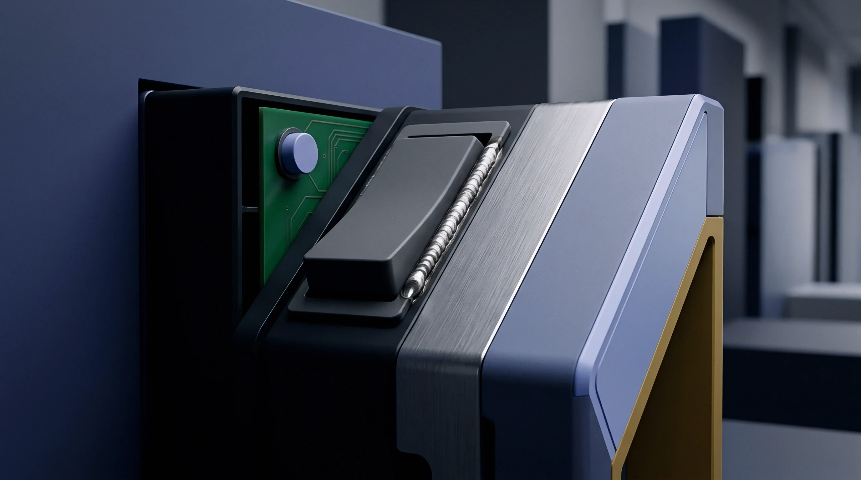
Resonant Frequency Formulations for Metallic Enclosures
Resonance calculations establish the exact frequency bands where cavity mode buildup threatens multi-radio isolation. Table calculations assume ideal conductive walls and uniform interior permittivity. Real housing builds introduce dielectric loading from FR-4 substrate materials, plastic lens carriers, battery packs, and internal cabling.
Dielectric loading lowers modal resonant frequencies relative to empty cavity predictions, shifting high-order modes down into active sub-6GHz radio channels.
Permittivity variations shift field peak distributions across the printed circuit board assembly. Adding high-density FR-4 circuit layers increases effective cavity permittivity, dropping modal frequencies by 15 percent to 35 percent compared to dry enclosure calculations. Field distributions compress spatially toward high-permittivity materials, concentrating electromagnetic energy directly within circuit board dielectrics.
Engineers must calculate both bare cavity modes and dielectric-loaded cavity modes to capture the full spectrum of potential internal coupling points.


Node
Standing wave patterns inside metallic casings establish fixed spatial locations where electric and magnetic field magnitudes reach local maximums. Spatial positions exhibiting peak electric field intensity are electric nodes, while positions exhibiting peak magnetic field intensity are magnetic nodes. Field distributions within sub-6GHz multi-transmitter enclosures create spatial coupling channels between components separated by several centimeters of physical circuit board distance.
Energy transfers efficiently when an unshielded trace or antenna feed aligns with peak field intensity locations. If a 2.4 GHz Wi-Fi power amplifier output trace sits directly beneath an electric field maximum of the TE110 cavity mode, power transfers out of the trace into the standing wave with minimal coupling loss. If a 5 GHz LNA input trace sits at another electric field maximum of a harmonic cavity mode, energy transfers out of the standing wave into the 5 GHz receiver chain.
Physical separation across the printed circuit board fails to provide spatial RF isolation when cavity modes bridge the gap.
Receiver sensitivity collapses. High-amplitude coupled RF energy drives low-noise amplifiers into gain compression, raising the receiver noise floor across active channels. When two sub-6GHz transmitters transmit simultaneously, cavity modes transport both fundamental signals into shared non-linear active stages, generating severe third-order intermodulation products.
Intermodulation signals generated inside the cavity fall directly into co-located receiver operating channels, causing severe receiver desensitization.
| Enclosure Dimensions (mm) | Target Sub-6GHz Band | Primary Excited Mode | Peak E-Field Location | Peak Coupling Factor (dB) |
|---|---|---|---|---|
| 100 x 80 x 25 | 5.8 GHz Wi-Fi 6E | TE320 Mode | Quarter-length interior coordinates | -8.2 |
| 150 x 100 x 40 | 3.5 GHz CBRS / 5G NR | TE210 Mode | Center-line across short housing axis | -11.5 |
| 200 x 150 x 50 | 2.4 GHz Wi-Fi / Bluetooth | TE110 Mode | Geometric center of primary PCB | -6.4 |
| 220 x 180 x 60 | 5.2 GHz Wi-Fi 6 | TE430 Mode | Grid matrix spaced every 27 mm | -14.1 |
| 300 x 200 x 80 | 700 MHz LTE / Sub-1GHz | TE110 Mode | Volumetric center of main cavity | -4.8 |
Quantifying peak field locations requires mapping spatial coordinate matrices against active sub-6GHz channel allocations. In a 150 mm by 100 mm by 40 mm enclosure, the TE210 mode at 2.23 GHz produces two prominent electric field peaks positioned at x = 37.5 mm and x = 112.5 mm along the 150 mm axis, centered along the 100 mm width. A Bluetooth or Wi-Fi transmitter trace laid across either coordinate experiences maximum coupling into the internal standing wave structure.
Moving sensitive trace runs away from calculated nodal coordinates recovers up to 25 dB of passive RF isolation without adding shielding hardware.
- Initial RF leakage from an unshielded power amplifier trace excites the fundamental cavity mode, transforming localized near-field energy into a high-amplitude standing wave across the housing interior.
- Resonant field buildup amplifies localized voltage gradients at spatial electric nodes, driving RF currents into adjacent printed circuit board ground planes and trace runs.
- Cross-radio injection delivers coupled signal energy directly into the low-noise amplifier input of a co-located receiver, exceeding front-end linear dynamic ranges.
- Systemic desensitization elevates receiver noise floors and generates intermodulation products that fail regulatory radiated spurious emission limits during formal certification scans.
Coupling severity scales with cavity quality factor Q. Unloaded metallic enclosures exhibit high Q factors ranging from 300 to 1,500 across sub-6GHz frequencies. High Q values mean electromagnetic energy accumulates over multiple RF clock cycles, resulting in narrow-band, high-amplitude field intensity peaks at exact mode frequencies. Loaded cavities containing lossy circuit components, battery structures, and absorber materials show lower Q values between 10 and 50.
Lower Q factors broaden resonant response bandwidth while suppressing peak electric field amplitudes, reducing total inter-chain power transfer.
Ignoring spatial node locations during component placement yields unrecoverable receiver desense that forces complete printed circuit board layout revisions late in product development.
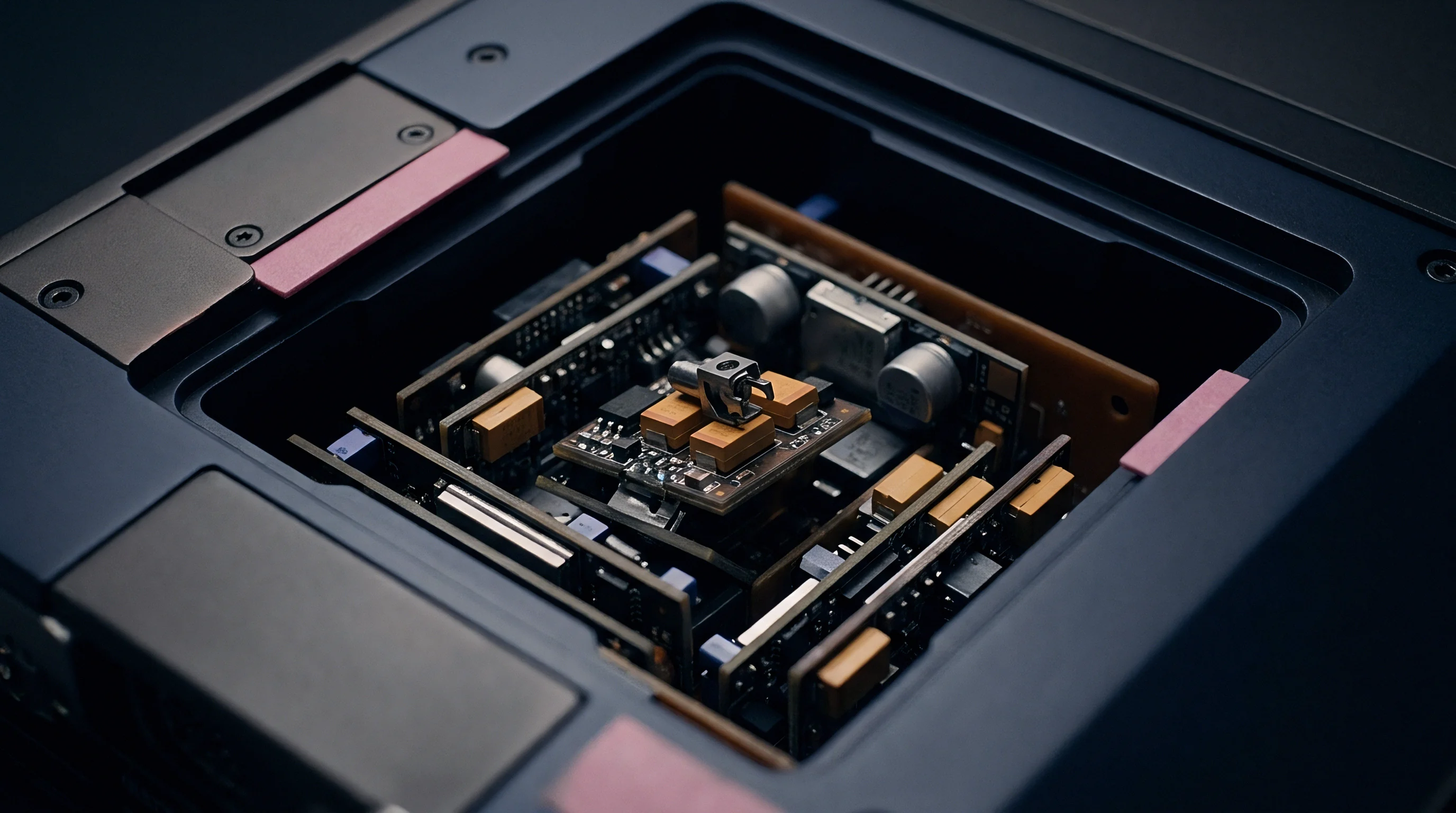
Spatial Distribution of Electric and Magnetic Highs
Standing wave structures exhibit discrete regional peaks separated by half-wavelength spatial intervals. Electric field nodes occur where magnetic field density reaches zero, while magnetic field nodes develop where electric field strength drops to zero. A magnetic field node positioned near a ground stitching via array induces strong RF loop currents into printed circuit board reference planes.
Ground plane noise then propagates into sensitive analog lines, phase-locked loop tuning nodes, and baseband clock traces.
Mapping spatial field distributions requires 3D full-wave finite-integration or finite-element electromagnetic simulation prior to layout freeze. Near-field magnetic probes scanned across an unshielded prototype inside an anechoic chamber reveal exact hot-spot locations. Comparing probe scan data against analytical mode models confirms whether field peaks stem from cavity resonances or localized microstrip radiation.
Distinguishing between cavity modes and trace radiation fixes the engineering resolution route.

RF Power Transfer across Co-Located Radio Chains
Power transfer between active sub-6GHz radios follows double-sided coupling formulations. The active transmitter trace acts as an excitation port driving the cavity mode, while the passive receiver trace acts as a receiving antenna extraction port. Power transfer efficiency peaks when both traces align with electric field nodes of the same resonant mode.
Under impedance-matched conditions, power transfer efficiency between co-located trace runs inside an unmitigated cavity can reach negative six decibels.
Decoupling co-located radio chains requires breaking field symmetry inside the housing. Rotating active trace geometry by 90 degrees relative to modal electric field vectors cuts energy transfer by 12 to 20 dB. Placing microstrip lines inside internal circuit layers bounded by continuous top and bottom copper ground planes shields trace signals from cavity modes.
Solid ground plane shielding prevents internal fields from establishing direct electric flux connections to signal conductors.

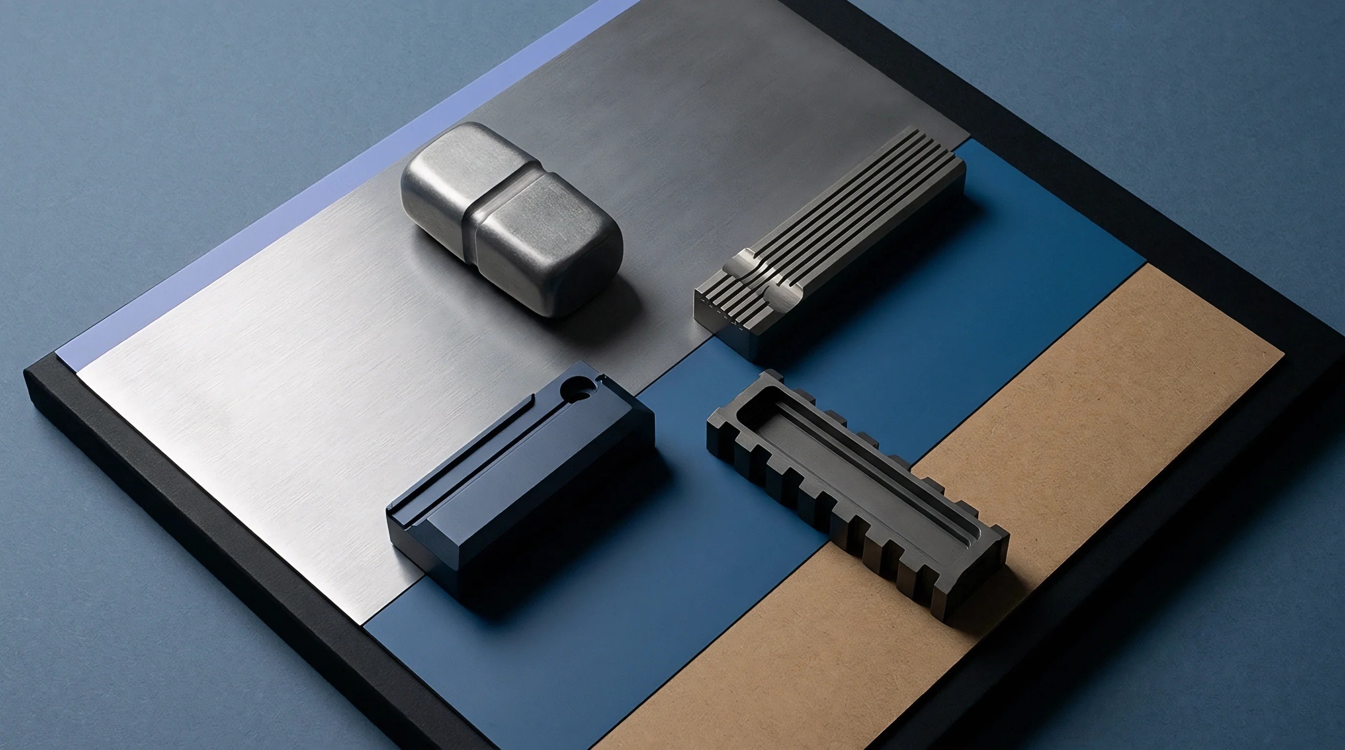
Absorption
Controlling internal electromagnetic fields inside dense housings requires introducing targeted dielectric and magnetic attenuation mechanisms. Dielectric loss and magnetic hysteresis dissipate standing wave RF energy into micro-watt thermal energy, damping internal field amplitudes. Dissipating internal field energy suppresses cavity quality factors, reducing cross-talk between co-located sub-6GHz radio modules.
| Material Composition | Thickness (mm) | Real Permeability at 5 GHz | Magnetic Loss Tangent | Q-Factor Reduction (dB) |
|---|---|---|---|---|
| Carbonyl Iron Elastomer Sheet | 0.50 | 2.1 | 0.45 | -12.4 |
| Sintered Ferrite Tile Sheet | 0.20 | 4.8 | 0.82 | -21.8 |
| Silicone Hybrid Flake Sheet | 1.00 | 1.8 | 0.38 | -9.6 |
| High-Permeability Magnetic Foam | 2.00 | 1.4 | 0.52 | -15.1 |
| Measurements conducted using a split-post dielectric resonator setup and 150 mm x 100 mm x 40 mm metallic calibration test fixture. | ||||
Applying thin lossy absorber sheets directly onto interior metallic walls converts high boundary magnetic field currents into thermal dissipation. Material selection depends on operational frequency bands. Synthetic elastomer materials loaded with carbonyl iron or planar ferrite flakes offer high magnetic permeability loss tangents across 1 GHz to 6 GHz.
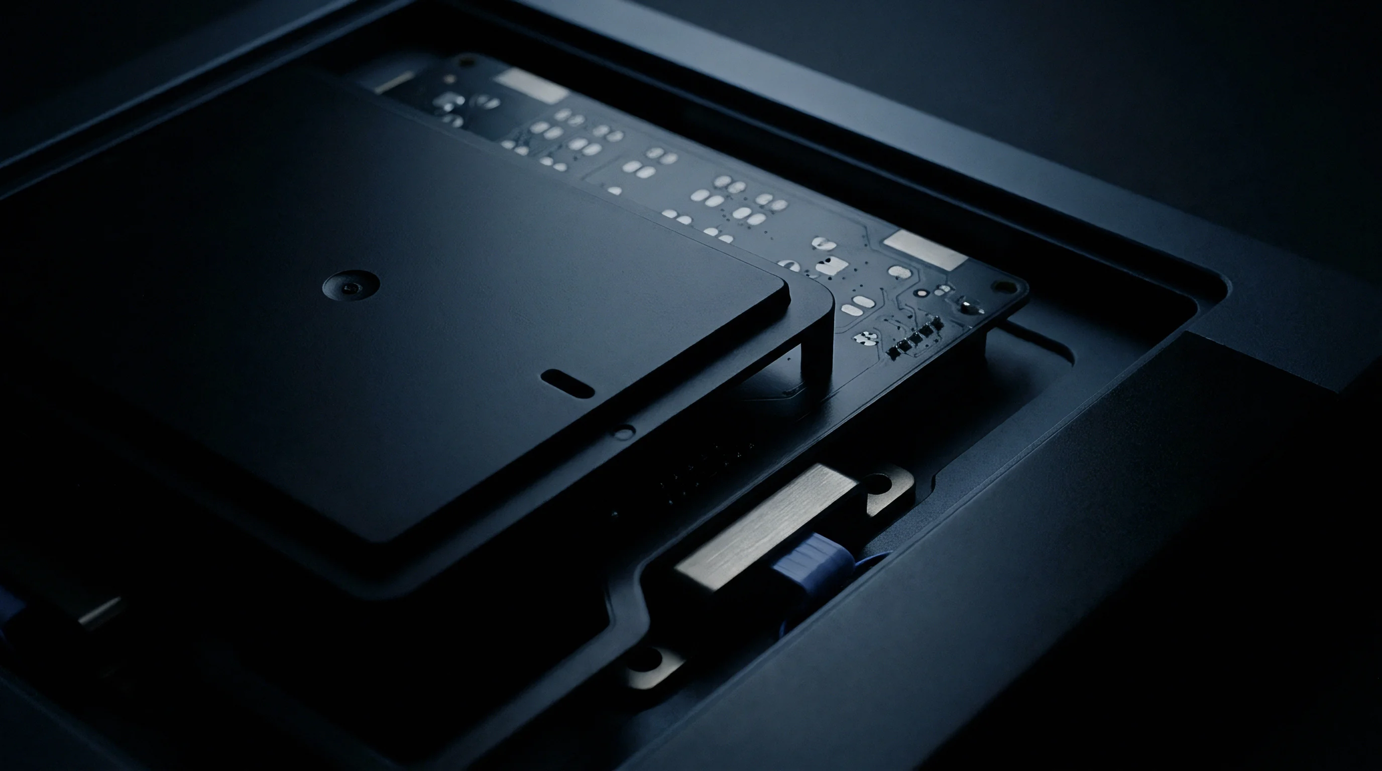
Attenuation performance peaks where magnetic field density reaches maximum levels, making interior enclosure ceilings directly above active radio modules prime application locations.
Compliance with ETSI EN 300 328 Clause 4.3.2.9 spurious emission limits mandates that internal cavity damping maintain harmonic leakage below negative thirty dBm per megahertz across all active operating combinations.
Dielectric absorbers rely on high electric permittivity loss tangents to attenuate electric field nodes. Carbon-loaded foam and conductive polymeric sheets dissipate energy when placed at spatial electric field maximums inside the volume. Placing dielectric absorbers directly over high-frequency microstrip lines can detune microstrip trace impedance, shifting 50-ohm signal paths to 38 ohms and degrading transmitter return loss.
Engineers must offset absorber positioning above high-speed trace lines to balance cavity Q damping against line impedance shifts.
- Thermal saturation drift occurs when high transmitter RF power heats magnetic absorber materials beyond their Curie temperature, causing sudden loss of permeability and rapid Q-factor escalation during long test cycles.
- Detuning frequency shifts happen when high-permittivity dielectrics placed too close to microstrip lines shift antenna trace impedance, creating severe return loss degradation and unexpected transmitter power reflected back into the enclosure cavity.
- Outgassing contamination degrades optical components and switches inside sealed housings when cheap unvulcanized elastomer backing materials release volatile organic compounds under continuous elevated operational temperatures.
- Adhesive layer shear separates surface-mounted absorption pads from enclosure walls during high-vibration qualification testing, allowing free-floating metallic-filled sheets to short power rails across the main printed circuit board assembly.
Strategic absorber placement relies on damping specific modal field nodes rather than lining entire internal enclosure surfaces. Lining entire interior walls increases material unit costs, adds mechanical weight, and risks thermal insulation build-up that elevates component junction temperatures. Placing a precise 20 mm by 20 mm square of magnetic absorber sheet directly over a calculated H-field node provides equal Q-factor reduction at five percent of the material cost.
Module vendors frequently claim that internal cavity resonances remain the sole responsibility of the host system integrator because shielding cans represent optional hardware accessories rather than certified assembly components.

Damping Sheet Properties and Material Loss Tangents
Flexible elastomer sheets impregnated with carbonyl iron or ferrite particles attenuate standing waves through magnetic hysteresis. Real permeability defines material ability to store magnetic energy, while imaginary permeability defines material ability to dissipate magnetic energy. The ratio of imaginary permeability to real permeability represents the magnetic loss tangent.
Materials with magnetic loss tangents exceeding 0.4 across target sub-6GHz frequencies deliver high attenuation per millimeter of material thickness.
Attaching absorber materials to interior surfaces requires pressure-sensitive acrylic adhesives rated for high continuous operating temperatures. Low-quality adhesives degrade under continuous thermal stress inside sealed multi-radio enclosures, causing absorber detachment. Detached absorbers float inside the cavity, exposing bare metallic walls, resetting cavity Q factors back to peak levels, and triggering sudden radiated emission test failures during formal compliance audits.
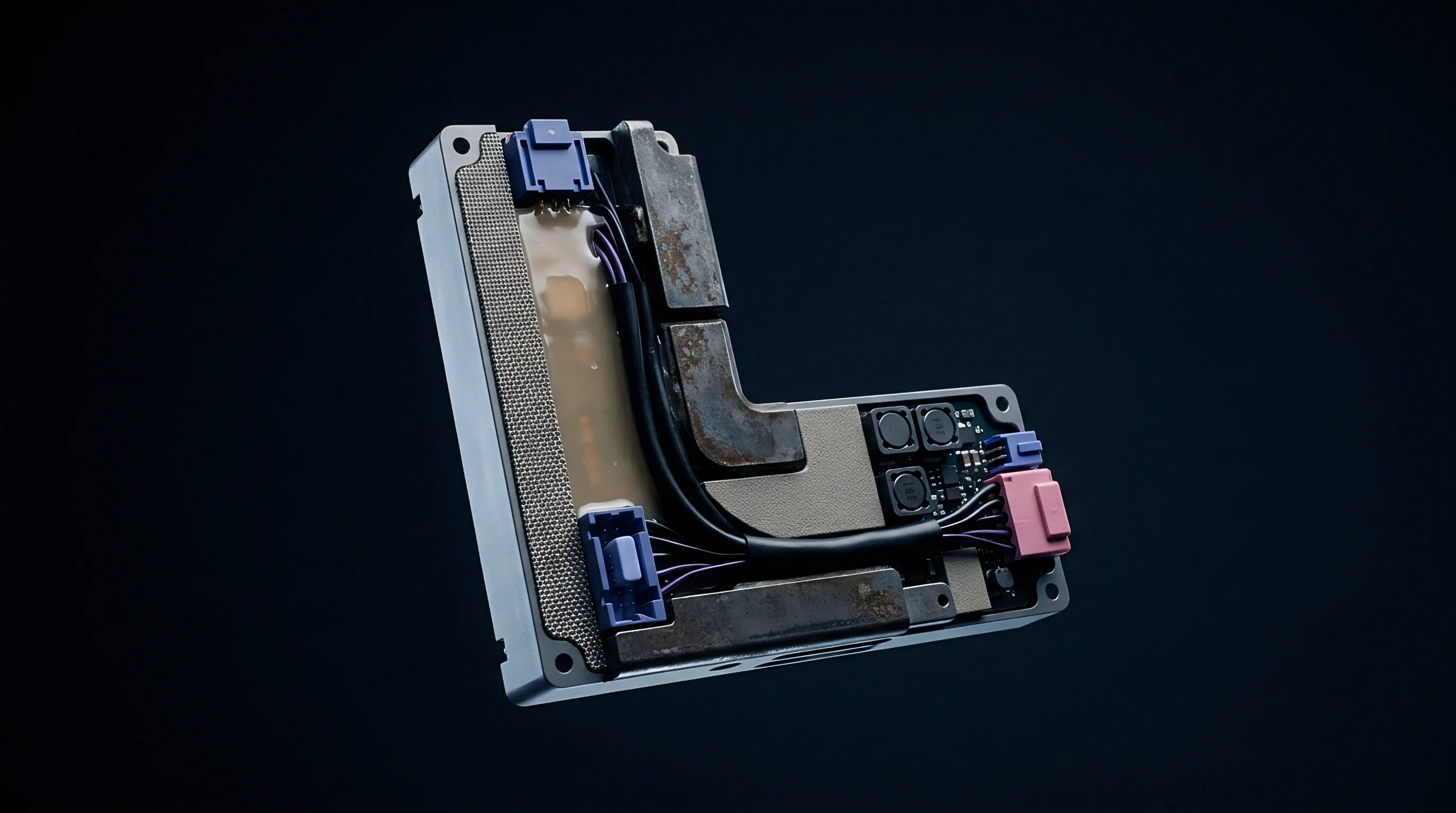
Enclosure Cavity Quality Factor Suppression Methods
Lowering the internal quality factor reduces peak electric field amplitudes across all active modes. Adding metallic partitioning walls inside the enclosure breaks single large cavities into smaller sub-cavities. Small sub-cavity dimensions push fundamental resonant frequencies upward, moving cavity modes above active sub-6GHz operating channels.
A sub-cavity measuring 40 mm by 30 mm by 15 mm exhibits a fundamental TE110 mode at 4.68 GHz, placing low-order resonances safely above 2.4 GHz Wi-Fi and 3.5 GHz 5G bands.
Partitioning wall effectiveness depends on ground stitching continuity where walls meet the main printed circuit board. Gaps in ground stitching act as slot antennas that leak energy between sub-cavities. Stitching via spacing along partition boundaries must remain below one-twentieth of a wavelength at the highest operating frequency.
At 7.125 GHz, maximum ground via pitch along partitioning shield walls must not exceed 2.1 mm to prevent inter-cavity leakage.

Coexistence
Simultaneous transmission across multiple sub-6GHz radios in a shared housing generates mutual interference pathways. Internal cavity modes act as high-efficiency distribution structures that route power from active transmitter output stages into co-located receiver low-noise amplifiers and adjacent transmitter power amplifiers. Multi-radio coexistence relies on suppressing cross-chain power transfer to preserve receiver sensitivity and prevent non-linear harmonic distortion during simultaneous operational modes.
| Regulatory Domain | Reference Standard | Frequency Range | Radiated Spurious Limit | Retest Trigger Threshold |
|---|---|---|---|---|
| United States (FCC) | FCC Part 15.247 / 15.407 | 30 MHz to 40 GHz | -41.3 dBm/MHz EIRP | 3 dB margin degradation |
| European Union (ETSI) | ETSI EN 300 328 / 301 893 | 30 MHz to 26 GHz | -30 dBm/MHz (>1GHz) | 2 dB margin degradation |
| Japan (MIC) | Radio Law Item 19 Article 2 | 30 MHz to 40 GHz | 2.5 uW/MHz (-26 dBm) | 2.5 dB margin degradation |
| China (SRRC) | Class II Radio Standard | 30 MHz to 12.75 GHz | -30 dBm/MHz | 3 dB margin degradation |
When transmitter RF power leaks into an adjacent active power amplifier via cavity modes, non-linear mixing occurs inside the final stage transistors. Third-order intermodulation products emerge at frequencies calculated as two times signal A minus signal B, and two times signal B minus signal A. If a 2.437 GHz Wi-Fi signal and a 2.4835 GHz Zigbee signal mix inside an unshielded cavity, intermodulation products land at 2.3905 GHz and 2.5300 GHz. These intermodulation signals radiate through housing seams and antenna elements, violating FCC Part 15 out-of-band emission limits.
Placing active multi-transmitter printed circuit traces orthogonal to cavity magnetic field lines minimizes energy transfer into internal standing waves.
Receiver desensitization measurements quantify isolation performance under active multi-radio stress conditions. LNA noise floor elevation occurs when cavity modes route transmitter broad-band phase noise and carrier leakage into the receiver front end. Injecting a 23 dBm transmitter signal into a cavity with 15 dB cross-chain isolation delivers 8 dBm of RF power directly to the co-located LNA input port.
This level exceeds the LNA 1 dB compression point, dropping receiver signal-to-noise ratios and causing packet error rates to spike.
- Measure individual transmitter output spectra on a conducted bench test set to establish baseline harmonic levels and phase noise profiles for each standalone radio module.
- Install the fully populated printed circuit board into the final enclosure housing without absorbing materials to identify unattenuated cavity mode frequencies using a near-field magnetic probe scan.
- Drive primary and secondary sub-6GHz transmitters simultaneously at full rated output power while monitoring the receiver low-noise amplifier input spectrum via a directional coupler.
- Position magnetic absorber sheet sections at identified peak field locations and iterate placement until cross-radio isolation exceeds thirty-five decibels across all operating channel combinations.
Harmonic generation multiplies coexistence challenges in multi-band sub-6GHz products. Second and third harmonics generated by a 2.4 GHz transmitter fall directly into the 4.8 GHz and 7.2 GHz bands. If cavity mode resonances align with these harmonic frequencies, harmonic energy amplifies within the cavity volume before coupling into 5 GHz and 6 GHz Wi-Fi receiver channels.
Suppressing harmonic excitation requires combining low-pass harmonic filters at transmitter output ports with cavity modal Q damping sheets.
Whether advanced three-dimensional electromagnetic simulation algorithms can reliably predict fine-grained internal cavity resonance coupling inside dense multi-layer flexible circuit builds without extensive physical chamber calibration remains open to debate among radio engineers.

Cross-Transmitter Intermodulation and LNA Desensitization
Coupling between active transmitter output stages forces non-linear mixing within power amplifier final transistors. Reverse isolation across modern integrated power amplifiers ranges between 15 dB and 25 dB across sub-6GHz frequencies. Internal cavity modes bypass amplifier reverse isolation pathways by delivering reverse drive signals directly to output matching networks.
Improving amplifier load impedance matching reduces intermodulation efficiency, suppressing third-order product generation by up to 10 dB.
Front-end LNA protection requires placing narrow-band surface acoustic wave or thin-film bulk acoustic resonator filters ahead of primary receiver input pins. Filters attenuate out-of-band coupled cavity signals before energy reaches active LNA transistors. Acoustic filters add 1.2 to 2.5 dB of in-band insertion loss, slightly degrading maximum free-space receiver sensitivity.
Product designers must trade off front-end insertion loss against multi-radio cavity desensitization immunity.

Harmonic Generation under Simultaneous Operating Modes
Multi-carrier excitation drives secondary harmonic frequencies into cavity modes aligned with high-band receiver channels. Harmonic emission amplitudes increase non-linearly with transmitter output power escalations. Operating a sub-6GHz transmitter at 27 dBm output generates harmonic levels 20 dB higher than operating the same transmitter at 20 dBm output.
Managing internal cavity harmonic coupling requires dynamic transmitter power back-off algorithms triggered whenever simultaneous multi-radio transmission occurs.
Transmitter power back-off reduces peak cavity field excitation levels during concurrent transmission cycles. Dropping transmitter output power by 3 dB cuts third-order intermodulation product amplitudes by 9 dB, restoring regulatory emission margins without mechanical design alterations. Dynamic power back-off routines must be embedded in firmware and validated inside fully equipped radiated measurement chambers across all target operational carrier combinations.


Clearance
Regulatory compliance certification for multi-radio products depends strictly on maintaining the physical layout evaluated during laboratory testing. Internal cavity resonances alter radiated spurious emission profiles, band-edge compliance margins, and total radiated power metrics. Certification grants issued by Telecommunication Certification Bodies under FCC rules or Notified Bodies under the EU Radio Equipment Directive bind host product designs to the exact mechanical build tested during formal qualification campaigns.
Modular grants specify precise shielding and antenna separation distances that bind host product designs. Integrating a certified modular radio into a new multi-transmitter enclosure alters the electromagnetic boundary conditions surrounding the module. Changing metallic wall distances or adding co-located transmitters invalidates the original modular grant assumptions.
Integrators must perform verification testing inside an accredited 3-meter or 10-meter semi-anechoic chamber to confirm host compliance under new enclosure boundary conditions.
Modifying internal metallic shielding or absorber pad thickness invalidates existing modular grant conditions and requires host compliance testing.
A compliance failure caused by internal cavity modes discovered during final certification scans creates expensive project delays. Retest schedules at accredited test laboratories run four to eight weeks out, while chamber hourly rates range from 300 to 600 dollars. Redesigning enclosure molds to alter cavity dimensions or add partitioning walls costs tens of thousands of dollars in tooling modifications and pushes product release dates past commercial launch windows.
Retests add four weeks. Chamber time grows costly. Sample counts double instantly.
Rejection follows quickly. Compliance margins disappear. Grants remain invalid.
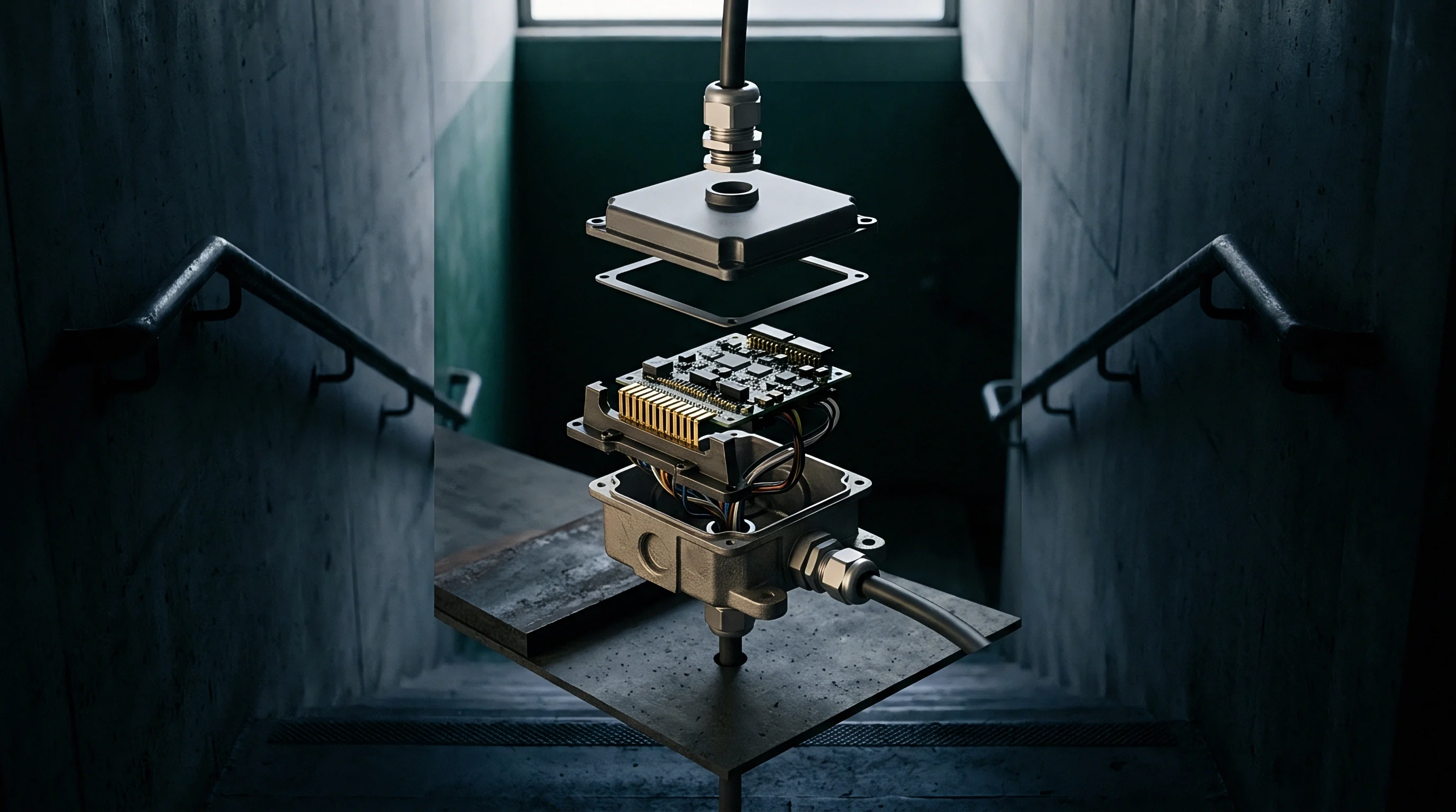
Documenting internal layout modifications for permissive change filings requires maintaining strict component trace records. Adding an absorber sheet, shifting board grounding screw positions, or adding conductive foam gaskets inside the housing represents a physical design change. Technical construction files submitted to regulatory agencies must contain exploded mechanical drawings, absorber material manufacturer datasheets, permeability specifications, and verified chamber measurement reports proving continued compliance.
FCC Part 2 Section 2.1043 Permissive Change rules mandate a Class II filing with full radiated spurious emission chamber data whenever internal housing modifications alter the radiated field profile by more than three decibels.
Host Integration Rules and Permissive Change Thresholds
Modular grants classify integration conditions into full modular approvals, limited modular approvals, and split-modular configurations. Full modular approval requires the radio module to possess its own metallic RF shielding cover. If a module vendor omits the RF shield cover to save costs, the grant converts to a Limited Modular Approval.
Limited approvals shift full radiated emission compliance responsibility onto the host system integrator, requiring full chamber qualification scans for every unique host enclosure design.
Permissive change classification depends on the magnitude of physical and RF performance alterations. Class I permissive changes cover minor modifications that do not degrade radiated spurious emissions or alter RF output power profiles. Class II permissive changes apply when physical layout modifications alter radiated field characteristics while keeping emissions within legal limit lines.
Changes that push radiated emissions over regulatory limits require invalidating existing approval identifiers and filing an entirely new grant application.

Regulatory Grant Conditions for Enclosure Modifiers
Altering internal metallic partitioning or damping sheet placement after initial approval triggers mandatory re-evaluation. Grant notes printed on official FCC certificates specify exact antenna separation distances, co-location limits, and operational duty cycles. If a host product enclosure places two modular radio antennas closer than 20 cm apart, standard standalone modular approvals no longer apply.
Co-located multi-transmitter evaluation protocols mandate simultaneous transmission radiated spurious emission testing under specific host grant authorization rules.
International regulatory acceptance varies across foreign trade jurisdictions. European Union CE marking under the Radio Equipment Directive 2014/53/EU relies on manufacturer Declarations of Conformity supported by ETSI EN 301 489-1 and EN 300 328 test dossiers. Japan MIC Giteki certification and China SRRC type approval require physical sample submissions for local in-country testing.
In-country testing laboratories evaluate products in their commercial shipping configurations, making unmitigated internal cavity resonances a primary cause of customs hold-ups and market entry denials.