Antenna Coupling Interference and Substrate Attenuation in Unlicensed Radio Modules
Host proximity near unlicensed module antennas degrades total efficiency and shifts harmonics over emissions thresholds requiring re-certification.


Coupling
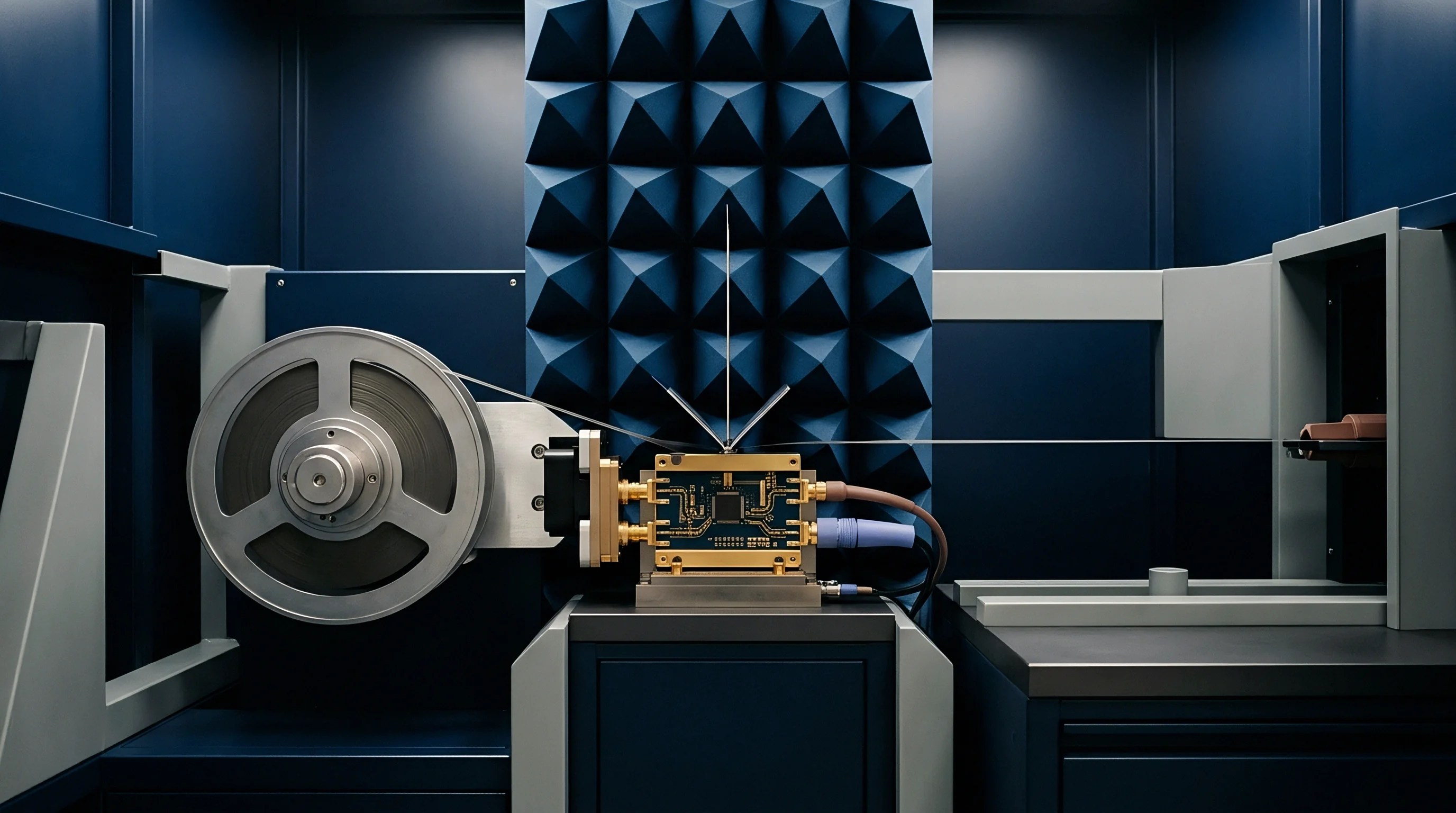
Rotational sweeps in a semi-anechoic chamber quickly expose how reactive fields interact with nearby metal. Operating a compact 2.4 GHz or 5.8 GHz radio module within millimeters of a host PCB, battery frame, or enclosure reshapes local electromagnetic boundary conditions. Radiators tuned in free space or characterized on reference ground planes suffer severe impedance pulling, pattern distortion, and parasitic radiation inside a real product chassis.
Near-field coupling turns passive traces and enclosure walls into secondary radiators, detuning the fundamental transmitter frequency and opening unintended paths for harmonics.
Coupling interference stems mainly from reactive near-field interactions within the space defined by a distance of R
An isolated antenna’s input impedance typically centers near 50 ohms resistive with zero reactance at resonance. Bringing host structures into close proximity introduces inductive or capacitive loading (+jX or -jX), driving the reflection coefficient $Γ = fracZin – Z0Zin + Z0 away from match. An antenna showing a standing wave ratio under 1.5:1 in free space can degrade past 3.5:1 when packed into a tight plastic shell beside a battery.
That mismatch reflects forward power back into the power amplifier, cutting total radiated power and degrading total isotropic sensitivity across the band.
This reactive loading detunes the radiator from its design frequency.
Engineers often mistake this mismatch for routine feed-line insertion loss, but the underlying issue is a shifted surface current distribution across the element. Uncoupled, currents follow designed vector paths along the arm to produce clean far-field lobes and predictable polarization. Placing a ground plane or battery shield in the reactive near-field induces opposing eddy currents that cancel radiated electric field vectors in specific polarizations, depressing total radiation efficiency and carving deep nulls into the field pattern.
A parasitic ground plane separation under 1.2 millimeters degrades antenna total radiation efficiency by 4.8 dB across the 5150 MHz to 5850 MHz band.
Near-field coupling also dumps fundamental and harmonic RF energy directly into adjacent digital traces. High-speed lines routed parallel to an unshielded antenna arm pick up this energy like receiving antennas. At full transmit power, the intense RF field induces interference voltages on power rails, sensor lines, and clock lines.
Traces carry this energy into non-RF circuitry, where non-linear semiconductor junctions rectify it. The resulting intermodulation generates spurious emissions that travel down cable harnesses and radiate during compliance scans.

Near Field Electromagnetic Interactions
Bringing conductors near a radiating element creates parasitic capacitive and inductive paths. Physical clearance determines whether energy transfers primarily through magnetic flux coupling or electric displacement currents. Microstrip, chip, and inverted-F antennas rely on controlled electric field lines between the radiator arm and underlying reference ground.
When host copper pours intercept these lines, energy bleeds into the system ground, adding parasitic capacitance that pulls down the resonant frequency.
The antenna’s input impedance shifts away from design targets as a result.
Magnetic coupling dominates when high RF currents at the base of a printed loop induce mutual currents in parallel host traces. Mutual inductance M12 between the antenna arm and a nearby trace scales with line length and inversely with the log of spatial clearance. If the host trace forms a closed loop, these currents circulate and dissipate transmit power as heat.
If the trace is open-ended, it acts as a parasitic monopole, re-radiating energy at unintended polarizations and elevation angles while distorting the overall radiation pattern.
An industrial handheld terminal housing a dual-band Wi-Fi module showed this behavior during evaluation. On the bare reference board, the printed inverted-F antenna exhibited a clean return loss profile. Inside the final assembly, a grounded copper ribbon cable feeding the thermal print head ran within 1.5 millimeters of the antenna tip.
The resulting parasitic capacitance pulled the 2.4 GHz resonance down to 2.28 GHz, shifting the entire 2400 MHz to 2483.5 MHz operating band off resonance. The standing wave ratio reached 4.2:1, forcing the power amplifier into thermal rollback and throttling network throughput.
Impedance Mismatch and Pattern Distortion
Energy reflected back toward the transmitter degrades radiated power and distorts the far-field pattern. Modern high-efficiency power amplifiers require specific load impedances to stay linear; impedance pulling shifts that load line and generates non-linear distortion. This distortion appears as spectral regrowth in adjacent channels, degrading adjacent channel leakage ratios and risking compliance failures under standards such as ETSI EN 300 328 and FCC Part 15.247.
Pattern distortion compromises intended spatial coverage.
An uncoupled radio module generally provides the uniform radiation pattern required for omnidirectional coverage. Near-field interactions introduce asymmetric phase shifts across the radiator aperture, pulling main beams toward internal metal or creating nulls in critical directions. In multi-antenna setups designed for spatial diversity or MIMO, coupling destroys spatial decorrelation between channels.
When elements couple through a shared host ground, cross-correlation coefficients climb, eroding MIMO multiplexing gains and link capacity in fading environments.
Diagnosing near-field coupling requires systematic isolation and measurement in a test chamber. Identifying these interactions before freezing the PCB layout avoids costly redesigns late in regulatory testing.
- Mount the unpopulated host board inside the calibrated 3-meter semi-anechoic chamber and calibrate the baseline antenna return loss using a vector network analyzer.
- Measure input impedance across the entire operational band from 2400 MHz to 2483.5 MHz to quantify resonant frequency shifting caused by bare board ground structures.
- Apply active power to adjacent high speed digital buses while monitoring near-field magnetic probes placed 2 millimeters above the printed antenna trace.
- Record radiated spurious emission sweeps on the automated turntable to identify parasitic harmonic tones elevated above the minus 41.2 dBm per MHz EIRP regulatory threshold.
- Solder decoupling components and ground stitching vias incrementally until the fundamental radiation pattern returns within 1.5 dB of the reference module datasheet.

Mutual Inductance in Unlicensed Bands
Operating in the 2.4 GHz and 5.8 GHz bands leaves printed trace antennas vulnerable to reactive crosstalk from high-speed digital lines. Modern host boards run interfaces with clock harmonics falling directly into these unlicensed allocations. Memory buses, display flex cables, and serial links emit broadband harmonic noise.
When routed near the antenna aperture, mutual coupling injects this digital noise straight into the receiver front end, degrading total isotropic sensitivity and reducing operational range.
Trace coupling causes severe receiver desensitization.
This drop in receiver performance from digital noise coupling into the antenna aperture is termed desensitization. In one hardware revision, a receiver rated for an intrinsic sensitivity of minus 98 dBm degraded to minus 82 dBm because an unshielded display flex cable ran alongside the module antenna. That 16 dB penalty cut effective operating range to a quarter of the design target.
Because the firmware interpreted the coupled energy as an elevated ambient noise floor, the issue produced no software error flags.
The extent to which transient ESD events near the antenna aperture degrade long-term dielectric performance without leaving visible burn marks remains an open question, particularly in high-humidity deployments.


Substrate
Relative permittivity and dielectric loss tangent dictate propagation velocity and signal attenuation along microstrip transmission lines. In unlicensed wireless modules, trace runs connecting transceivers, matching networks, filters, and antenna feeds rely on the PCB substrate to deliver RF power cleanly. Selecting the wrong laminate or failing to account for dielectric drift across temperature introduces loss long before energy reaches the antenna.
Signal attenuation in a PCB substrate comes down to two loss mechanisms: conductor loss Ac driven by finite copper conductivity and surface roughness, and dielectric loss Ad governed by substrate dissipation factors. The dielectric attenuation coefficient for a microstrip line is given in decibels per unit length by:
αd = 27.3 · fracvarεrsqrtvarεeff · fracvarεeff – 1varεr – 1 · fractanδλ0 quad dB/m
Here, varεr is relative dielectric permittivity, varεeff is the effective dielectric constant of the microstrip geometry, tanδ is the dissipation factor, and λ0 is the free-space wavelength. Moving up into the 5.8 GHz and 6 GHz Wi-Fi 6E/7 bands shortens λ0, driving dielectric attenuation up linearly with operating frequency.
Standard FR-4 glass-epoxy remains common in low-cost builds because it is inexpensive and simple to process. However, FR-4 exhibits a loss tangent of 0.015 to 0.022 at 2.4 GHz, worsening to 0.020 ~ 0.028 at 5.8 GHz. These high dissipation factors turn printed traces into attenuators that convert transmitter output into core heat.
A 20-millimeter microstrip trace on standard FR-4 at 5.8 GHz can absorb over 1.2 dB, dissipating more than 24 percent of the RF energy as heat before it reaches the antenna feed.
Dielectric losses scale up aggressively with frequency.
Copper surface roughness pushes losses well past smooth-copper theoretical limits. Multilayer PCB fabrication relies on chemical micro-etching to bond copper foil to prepreg layers. At microwave frequencies, current crowds into a thin skin depth along the copper surface, where tooth profile variations force current along longer paths through microscopic peaks and valleys.
Copper skin depth measures roughly 1.33 micrometers at 2.4 GHz and shrinks to 0.86 micrometers at 5.8 GHz. When root-mean-square surface roughness Rq exceeds skin depth, conductor attenuation jumps 30 to 60 percent over smooth-copper calculations.
| Substrate Material | Relative Permittivity (varεr) | Loss Tangent (tanδ) | Attenuation at 2.4 GHz (dB/cm) | Attenuation at 5.8 GHz (dB/cm) | Phase Velocity Factor |
|---|---|---|---|---|---|
| Standard FR-4 Epoxy | 4.40 | 0.0200 | 0.18 | 0.52 | 0.54 |
| High-Tg FR-4 (370HR) | 4.17 | 0.0160 | 0.14 | 0.41 | 0.56 |
| Hydrocarbon Ceramic (RO4350B) | 3.48 | 0.0037 | 0.04 | 0.11 | 0.61 |
| PTFE Woven Glass (RO5880) | 2.20 | 0.0009 | 0.01 | 0.03 | 0.72 |
| Modified Polyimide Flex | 3.20 | 0.0050 | 0.06 | 0.16 | 0.63 |
Moisture absorption presents another operating hazard for field hardware. Glass-epoxy laminates absorb 0.30 to 0.50 percent of their dry weight in water under humid ambient conditions. At microwave frequencies, water exhibits a high relative permittivity (varεr ≈ 78) and a steep loss tangent (tanδ ≈ 0.15).
Water ingress increases both the dielectric constant and dissipation factor of the board, detuning matching networks and altering phase velocity through embedded filters.

Dielectric Dissipation and Skin Depth Effects
Transmission line attenuation rises rapidly as operating frequencies extend into the upper gigahertz range. The skin effect confines current flow to a thin outer boundary layer along the trace conductor. Skin depth δ is calculated as:
δ = sqrtfracρπ f μ0 μr
Where ρ is electrical resistivity, f is frequency, μ0 is free-space permeability, and μr is relative permeability of the conductor. As skin depth contracts at higher frequencies, the effective cross-sectional area for current shrinks, increasing AC line resistance and insertion loss per unit length.
Surface roughness elevates these conductor losses further.
Combining skin depth contraction with high dielectric loss makes laminate selection a critical decision for unlicensed RF designs. Relying on standard FR-4 at 5.8 GHz or 6 GHz introduces substantial feed-line loss, forcing the power amplifier to draw more current to maintain target output. Driving the amplifier harder increases thermal loading and battery consumption while elevating harmonic distortion, complicating radiated emissions compliance during full-power testing.

FR-4 Limitations versus High Frequency Laminates
Standard glass-epoxy resins carry high dissipation factors that absorb RF energy before it reaches the radiator. Upgrading to ceramic hydrocarbon or PTFE-based laminates lowers dielectric loss and stabilizes relative permittivity across broad temperature and frequency ranges. These high-frequency materials maintain loss tangents below 0.004, preserving RF power and holding transmission line impedance stable across operational channels.
Substrate choice directly governs compliance headroom and thermal behavior under continuous operation.
- Permittivity dispersion alters transmission line impedance, creating discontinuities that reflect power back toward the amplifier.
- Moisture absorption loss increases dielectric dissipation in humid environments, pulling transmit power down by up to 2.3 dB.
- Copper surface roughness conductor attenuation restricts skin-depth current paths, raising resistive losses on narrow printed traces.
- Thermal loss tangent expansion shifts patch radiator resonance downward during long, continuous transmit bursts.
A batch of compact 5.8 GHz sensor nodes fabricated on high-Tg FR-4 demonstrated this vulnerability by failing coverage tests during tropical field deployments. Bench tests in a dry lab showed an acceptable 0.45 dB insertion loss between the module output pin and the antenna feed. Placing the assemblies in a humidity chamber at 85 percent relative humidity increased dielectric loss, raising line attenuation to 1.65 dB.
That additional 1.2 dB loss reduced effective range by 25 percent, requiring a board re-spin onto hydrocarbon ceramic laminate to stabilize performance.

Environmental Moisture Absorption and Thermal Shifts
Absorbed moisture alters a PCB’s effective permittivity, pulling center frequencies off target. Temperature-induced dielectric variations also generate phase shifts along feed networks, degrading beamsteering accuracy and phased-array calibration. Standard FR-4 exhibits a thermal coefficient of dielectric constant (TCvarεr) between +100 and +250 p±/circC, whereas high-frequency hydrocarbon laminates maintain TCvarεr within ± 40 p±/circC.
Compliance with ETSI EN 300 328 Clause 4.3.2.9 requires radiated spurious emissions to remain below minus 30 dBm for frequencies exceeding 1 GHz during active transmission.
High duty cycle packet transmissions generate localized heating around power amplifier outputs. These thermal gradients expand the dielectric matrix and alter local permittivity, pulling matching networks off resonance. The resulting thermal detuning increases insertion loss during extended packet bursts, degrading throughput during high-bandwidth transfers.
Routing microstrip feeds with ground plane clearances greater than three times the substrate thickness helps prevent near-field capacitive pulling during integration.

Harmonics
Non-linear behavior in RF front-end amplifiers interacts with parasitic coupling to convert fundamental carrier energy into harmonic frequencies. Operating an unlicensed radio module at full output power drives power amplifier non-linearities, generating harmonics at integer multiples of the fundamental (2f0, 3f0, 4f0). On a standalone module, internal filtering holds these harmonics below regulatory limits.
Once integrated into a host device, parasitic coupling and substrate surface waves can bypass shielding, launching harmonic currents into host metal that acts like an unintended antenna array.
Radiated harmonic emissions represent a common compliance bottleneck during market approval testing under FCC Part 15 Subpart C and the European Radio Equipment Directive. FCC Part 15.247 rules for 2.4 GHz digital modulation systems require out-of-band spurious radiation to stay below strict field strength limits at a 3-meter measurement distance. Above 1000 MHz, the general limit is 54 dBμV/m average EIRP (equivalent to -41.2 dBm) and 74 dBμV/m peak EIRP (-21.2 dBm).
Compliance margins frequently degrade during host-level integration testing.
When the antenna couples into host copper, the radiator’s effective aperture expands to encompass the host ground plane, battery casing, and display shield. The module’s internal filter may attenuate second harmonics by 45 dB relative to the carrier at the output pad, but near-field coupling off the antenna trace bypasses that filter. Fundamental energy couples into host metal, where non-linear junctions or mechanical contact points re-radiate second and third harmonics into free space, exceeding regulatory limits.
| Regulatory Agency | Band Standard | Radiated Spurious Limit | Permissible Antenna Gain Shift | Permissive Change Category |
|---|---|---|---|---|
| FCC (United States) | Part 15.247 / 15.407 | -41.2 dBm/MHz Average EIRP | Equal or Lower Peak Gain | Class II Permissive Change (C2PC) |
| ISED (Canada) | RSS-247 Issue 3 | -41.2 dBm/MHz Average EIRP | Same Type, Equal/Lower Gain | Class 4 Permissive Change (C4PC) |
| ETSI (Europe) | EN 300 328 / EN 301 893 | -30 dBm/MHz Peak EIRP (>1GHz) | Re-assessment Required | Host DoC Technical Construction File Update |
| MIC (Japan) | Giteki Radio Law Art. 2 | -26 dBm/MHz EIRP Spurious | No Increase Permitted | Type Certified Host Amendment |
When antenna coupling generates harmonic spikes or degrades primary radiation patterns, the integration invalidates the original modular grant conditions. Modular hardware streamlines certification only when layout guidelines are followed precisely. Altering antenna trace routing, changing enclosure spacing, or placing modules near internal metal voids baseline test conditions, obligating host manufacturers to submit updated compliance documentation.

Parasitic Radiated Spurious Emissions Mechanics
Traces routed near an unshielded antenna pick up high-frequency energy and function as secondary parasitic radiators. High-intensity electric fields from the fundamental induce surface currents on adjacent host wiring. These currents travel along unshielded conductors until they reach impedance discontinuities ~ such as connector interfaces or enclosure seams ~ where they radiate into free space.
These unintended radiation mechanisms regularly lead to test failures.
Re-radiated harmonic energy tends to be highly directional. While the fundamental signal follows an intentional, broad radiation pattern, second and third harmonics radiate in narrow, irregular lobes. On an automated test chamber turntable, these lobes can exceed compliance thresholds at specific rotation angles and antenna heights, causing compliance failures despite compliant conducted measurements on the bench.

Permissive Change Classifications and Scope
Modifying antenna ground dimensions or altering enclosure metal triggers specific filing obligations under international approval rules. Under FCC modular frameworks, integrating a module into a host with altered antenna trace geometry, alternate antenna types, or higher peak gain requires formal filings ~ typically a Class II Permissive Change supported by accredited laboratory test reports.
Correctly classifying and executing these filings prevents product launch delays.
Under ETSI EN 300 328 standards for the European market, host integrations cannot rely solely on module-level declarations if mechanical placement alters radiated performance. The host manufacturer bears legal responsibility for ensuring the completed product meets radiated spurious limits, requiring radiated pre-scans and technical construction file updates prior to applying the CE mark.

What Triggers a Mandatory Re-Certification for Host Antenna Coupling Alterations?
Regulatory bodies enforce strict limits on antenna gain variations and physical layout changes within host enclosures. Deviating from certified reference designs invalidates existing modular approvals and mandates formal filing actions. Identifying these trigger conditions during initial layout prevents unplanned re-certification costs prior to production ramps.
- Antenna trace geometry review confirms whether physical line dimensions match the approved grant file within a 5 percent physical margin.
- Ground plane clearance measurement verifies that enclosure boundaries maintain required physical separation from active radiating elements.
- Radiated spurious pre-scan evaluation checks harmonic levels against Class II permissive change filing trigger thresholds prior to submission.
- RF exposure co-location assessment calculates combined SAR contribution when auxiliary wireless transmitters operate simultaneously inside the host.
Ground plane continuity unbroken by digital routing traces prevents parasitic return current loops from forming secondary radiator loops.
An unshielded display flex cable coupling into a 5.8 GHz antenna pushed radiated harmonics 3.4 dB over the FCC Part 15 Class B ceiling during integration testing, resulting in a twelve thousand dollar re-test cost and a four-week launch delay.


Layout
The physical arrangement of grounding vias, trace spacing, and shield enclosures dictates the electromagnetic isolation achievable on multilayer PCBs. Isolating sensitive RF feeds from high-speed digital lines while controlling near-field antenna interactions requires strict layout discipline. Guard traces, shielding enclosures, and controlled-impedance geometry together limit substrate attenuation and coupling interference across operational bands.
Coplanar waveguide with ground (CPWG) structures provide tighter field confinement than standard microstrip when routing RF lines through dense board layouts. CPWG places grounded copper pours on both sides of the center RF trace on the top layer, backed by a continuous reference ground directly below. These side ground pours contain electric field lines that would otherwise fringe into adjacent board areas, preventing near-field coupling into neighboring traces or enclosure walls.
Solid reference ground copper suppresses unwanted board resonance modes.
Designing a CPWG line requires sizing trace width w and gap clearance s to hit a 50-ohm characteristic impedance target. CPWG impedance depends on relative permittivity and geometric ratios evaluated using complete elliptic integrals of the first kind K(k):
Z0 = frac3772 sqrtvarεeff · fracK(k’)K(k)
Where k = fracww + 2s and k’ = sqrt1 – k2. Narrowing the gap s concentrates the electric field in the air space above the trace, reducing reliance on substrate loss tangents and lowering dielectric dissipation in the board material.
Stitching via fences along CPWG side grounds suppresses substrate modes and prevents parallel-plate resonances across multilayer stackups. Spacing stitching vias closer than one-tenth of the guided wavelength (λg / 10) forms an effective electromagnetic wall. At 5.8 GHz, ground via pitch must remain under 2.8 millimeters; wider spacing allows surface waves to propagate through internal layers, coupling RF energy into analog sensor lines or digital buses.

Coplanar Waveguide Design and Guard Vias
Flanking conductors with ground pours and dense via stitching confines electric fields within the local dielectric. Guard vias provide a low-impedance return path directly alongside the signal line, minimizing current loop area and reducing magnetic dipole radiation from the printed trace.
Surface-mounted shielding cans contain near-field electromagnetic emissions.
Placing metal shields over active transceivers and matching networks limits near-field magnetic coupling to surrounding components. A solder-mounted shield acts as a Faraday cage around RF circuitry, containing internal fields while blocking digital switching noise from reaching the receiver front end. Shield cans require continuous perimeter solder joints to prevent aperture gaps that act as slot radiators at microwave frequencies.

Enclosure Metallic Boundaries and Far Field Effects
Metal housings located within the reactive near-field absorb radiated energy and distort primary beam directivity. Plastic enclosures treated with conductive anti-static coatings create similar degradation if placed too close to the radiator. Conductive coatings present surface resistivities that dissipate near-field energy as heat, lowering radiation efficiency without providing true far-field plane wave shielding.
Enforcing physical clearance boundaries preserves antenna radiation efficiency.
Maintaining a keep-out zone clear of copper pours, internal hardware, and metal fasteners is necessary to protect far-field pattern symmetry. Keep-out clearances should extend at least 15 millimeters around 2.4 GHz radiating elements and 10 millimeters for 5.8 GHz modules. Maintaining these clearances holds input impedance within 5 percent of target specifications, preventing detuning and avoiding the expense of compliance re-testing during certification.

Ground Plane Stitching and Isolation Channels
Providing uninterrupted ground copper beneath the module interface stops common-mode return currents from circulating through the system ground. Slotting or segmenting ground planes under RF paths creates impedance discontinuities that force return currents around slot boundaries, forming loop structures that radiate spurious energy. Continuous reference ground planes under RF traces maintain stable characteristic impedance and preserve signal integrity across the operating band.
Shielding cans placed over active RF circuitry reduce near-field magnetic coupling to host traces by more than 25 dB.
When board area is constrained, routing isolation moats through host ground fills helps separate noisy digital switching circuits from sensitive RF grounds. These channels prevent ground bounce from propagating across multilayer boards, protecting receiver sensitivity across all channels. Combining isolation channels with grounded via fences provides a robust layout architecture, ensuring unlicensed modules meet link budget targets and pass regulatory scans.