Host Board Layout Constraints during Secure Element Modular Radio Integration
Placing secure elements near modular radios demands ground isolation, trace impedance control, and shielding to preserve transmitter compliance and pass radiated pre-scans.
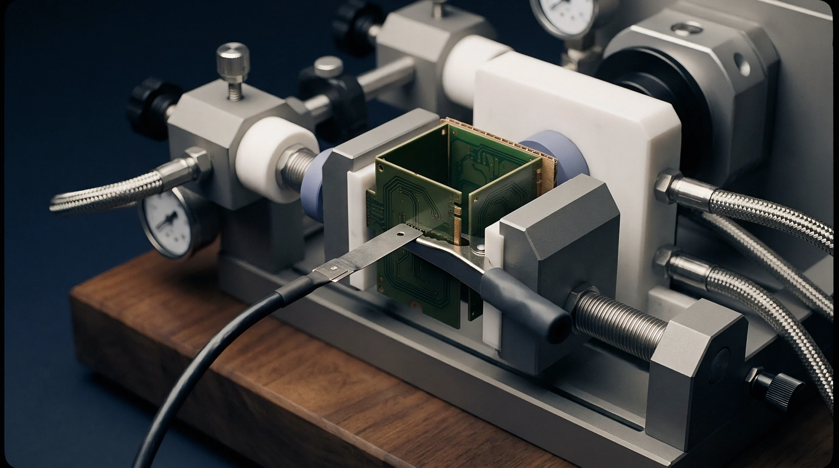

Proximity
Inside an anechoic chamber, a spectrum analyzer trace shows the effect of spatial crowding almost immediately. Placing a secure element integrated circuit within 15 millimeters of a modular radio front-end lets high-frequency digital clock harmonics bleed straight into the receiver low-noise amplifier. During radiated emissions pre-scans under ETSI EN 300 328, unshielded serial peripheral interface lines running at 40 megahertz generate spurious peaks within 1.5 decibels of the regulatory threshold.
As the turntable rotates three hundred and sixty degrees, the peak remains above ambient floor noise across all antenna polarizations, forcing layout changes well before formal filing submission.
Host printed circuit board designs require strict physical separation between cryptographic integrated circuits and modular radio components. Secure elements draw transient currents during public-key operations, such as elliptic curve scalar multiplication. These current spikes, occurring at frequencies from 10 megahertz to 100 megahertz, create localized electromagnetic fields.
Routing these signal currents alongside a 2.4 gigahertz or 5 gigahertz modular radio antenna feedline causes inductive and capacitive cross-talk. Nearby power amplifier thermal paths can also create temperature gradients across the board, degrading the clock oscillator stability of adjacent secure hardware.

Host Clearance Bounds near Module Perimeters
Mounting a modular radio assembly on a host board sets physical boundaries that govern trace layout within surrounding copper layers. Modular certification grants under FCC Part 15.247 assume specific antenna keepout areas, typically extending at least 20 millimeters beyond the module edge or trace antenna. Placing secure element chips, high-speed security buses, or external cryptographic memory modules inside this keepout zone alters the radiation pattern of the module’s integrated antenna.
Distance between high-speed serial buses and radio front-ends prevents destructive harmonic coupling in receiver bands.
Because antenna keepout zones dictate layout, running high-speed digital logic beneath a module metal shield triggers near-field capacitive coupling through the host fiberglass substrate. This coupling shifts the resonant frequency of internal antenna structures, causing impedance mismatches that lower total radiated power while elevating unwanted harmonic emissions.
Physical interference profiles differ across integration architectures, revealing distinct spatial failure modes during board bring-up:
- Antenna Feedline Overlap occurs when high-frequency serial clock lines pass beneath modular radio microstrip routing, injecting digital noise directly into the transmitter path.
- Secure Element Power Plane Contamination develops when cryptographic acceleration units draw transient currents from a shared system voltage rail without adequate low-pass filtering.
- Ground Edge Refinement Deficits manifest when secure chip ground vias connect directly to the perimeter copper poured under a modular radio antenna system.
- Thermal Gradient Shift occurs when high-power cellular modular radios transfer thermal energy into adjacent secure elements, destabilizing internal real-time clocks.
Placing components without calculating spatial clearance forces engineering teams to scrap initial host prototypes, re-spin four-layer or six-layer boards, and reschedule reserved test chamber slots at high financial cost, delaying commercial launch.

Stackup
Layer arrangement within a multi-layer host board forms the primary defense against internal electromagnetic interference between security hardware and radio modules. A standard six-layer stackup assigns layer one to RF microstrip routing and modular solder pads, with layer two serving as a continuous ground reference plane. Placing high-speed SPI or ISO 7816 bus signals on layer three without solid reference copper above and below subjects those lines to strong electromagnetic fields radiated from the modular transceiver above.
Ground plane continuity beneath both the secure element package and the modular radio must stay unbroken by signal vias or split power planes.
Continuous ground planes directly beneath modular radios reduce radiated spurious emissions by over 12 decibels under ETSI EN 301 489-1 testing conditions.

Reference Plane Selection for High Frequency Traces
Microstrip routing on external layers requires precise dielectric thickness calculations to maintain controlled 50-ohm single-ended impedance for RF paths and 90-ohm differential impedance for secure communication lines. Stripline routing embedded between two solid ground planes on internal layers isolates secure element data lines from radio frequency energy radiated by the module. Standard FR-4 glass-reinforced epoxy substrates present a relative permittivity of approximately 4.3 at 2.4 gigahertz, though dielectric losses increase at higher frequencies.
Controlled impedance fabrication specifications prevent signal reflections along trace pathways, preserving signal integrity across both RF feedlines and cryptographic buses.
| Interface Type | Trace Impedance Target | Minimum Clearance to RF Feed | Maximum Permitted Length | Primary Failure Mode |
|---|---|---|---|---|
| RF Antenna Feedline | 50 ohms +/- 5% single-ended | Reference boundary | 15 mm | Mismatched return loss and elevated VSWR |
| Secure Element SPI Bus | 50 ohms single / 100 differential | 12.5 mm | 50 mm | Spurious emission peaks at clock harmonics |
| Secure Element ISO 7816 | 50 ohms single-ended | 15.0 mm | 75 mm | Transient noise causing reset line triggers |
| I2C Security Bus | Open-drain / 50 ohms match | 10.0 mm | 40 mm | RF rectification into serial data lines |
Designing host boards without strict dielectric height tolerance specifications allows trace impedance to drift rapidly, causing variations exceeding 15 percent across manufacturing batches that degrade RF output power and receiver sensitivity.

Differential Clock Routing under RF Shields
Cryptographic microcontrollers frequently utilize high-frequency external oscillators to execute side-channel attack countermeasures and rapid cryptographic operations. Routing these differential clock signals across board layers demands a structured procedure to guarantee signal containment and regulatory compliance:
- Route differential clock pairs on an internal layer situated between two unbroken ground reference planes.
- Maintain a constant inter-trace distance equal to the trace width to lock differential impedance at the target specification.
- Surround the clock trace pair with ground stitching vias spaced at intervals no greater than one-tenth of the highest harmonic wavelength.
- Terminate differential trace lines with precision surface-mount resistors directly at the receiver pins of the secure element.
- Verify that no signal vias transition the clock line across different reference layers along its route.
Solid copper ground layers beneath high-frequency components contain near-field electromagnetic radiation within the internal board structure. Omitting continuous ground planes under the radio module host footprint creates high-impedance return paths that act as unintentional slot antennas, emitting broad noise bands during compliance testing.


Coupling
Interference transfers between host components through conductive paths, inductive loops, and capacitive field interaction. When a cellular module transits into maximum transmit power mode during carrier connection bursts, current draw spikes by up to 2 amperes across a few microseconds. This sudden power drop propagates along shared power supply lines, inducing transient voltage ripples into the supply pins of adjacent secure element chips.
Secure chips subjected to supply ripple experience clock jitter and internal brown-out resets, halting active cryptographic sessions.
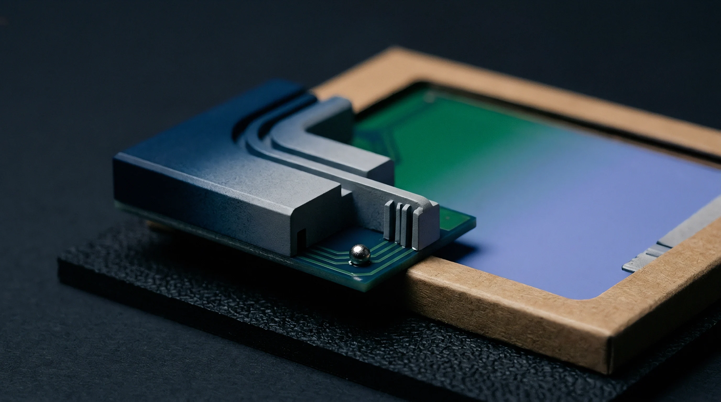
Which PCB Layer Stackup Prevents Secure Element Bus Crosstalk?
Stripline stackup configurations placing signal lines between two ground planes eliminate high-frequency crosstalk between secure element data lines and modular transceivers. A five-layer or six-layer board structure using inner layers for digital bus routing shields sensitive signals from radiated RF fields generated by top-mounted modular antennas. Capacitive coupling between top-layer RF traces and inner-layer digital traces drops below minus 60 decibels when an intervening ground plane remains solid and unslit beneath the entire module footprint.
Trace layout geometry directly dictates mutual inductance levels between adjacent signal paths. Consider an unshielded 3.3-volt serial clock line running parallel to a 50-ohm RF microstrip line for a length of 25 millimeters with a center-to-center spacing of 0.8 millimeters. The mutual capacitance per unit length under standard FR-4 dielectric parameters yields approximately 0.12 picofarads per centimeter.
At an operating frequency of 2.45 gigahertz, this capacitance introduces a low-impedance path that couples 18 millivolts of RF voltage directly into the digital clock receiver. The coupled RF signal rectifies inside the secure element input stage, shifting the digital logic threshold and triggering false bus frame errors.
FCC Part 15.247 radiated spurious emission rules mandate that all field strength emissions above 960 megahertz remain below 54 dBuV/m at a 3-meter test distance.

Decoupling Capacitor Loops and Power Supply Noise
Decoupling network design dictates power rail purity across the host assembly. Low equivalent series resistance ceramic capacitors placed near secure element power pins sink high-frequency noise currents to ground before they enter signal traces. Spurious noise propagation worsens when decoupling capacitor ground vias connect to reference planes through long, high-inductance traces.
Software filtering or lower clock rates are sometimes assumed to eliminate the need for trace isolation around secure elements, but that perspective collapses in the test chamber when radiated scans show strong clock harmonics breaching limits regardless of firmware. Short, wide surface traces and ground vias reduce parasitic inductance, connecting decoupling capacitors directly to secure element power pins to maintain power stability across all operating modes.


Shielding
Physical metallic barriers mounted on the host board contain stray electromagnetic emissions and protect cryptographic circuitry from external physical tampering. Metal shield cans soldered over host secure element clusters create a Faraday cage that attenuates incoming radio frequency energy from adjacent modular radios. The effectiveness of a shield enclosure depends on ground pin spacing along its perimeter, solder joint integrity, and aperture sizes designed for thermal ventilation.

Physical Tamper Enclosures near Modular Antenna Keepouts
High-security integrations, such as point-of-sale terminals and secure identity gateways, demand physical tamper protection compliant with FIPS 140-3 Level 3 or Common Criteria EAL6+ standard criteria. These physical security mechanisms utilize active mesh layers embedded within the PCB structure or conductive enclosure covers that detect drilling or probing attempts. Placing metallic mesh layers near modular radio antennas alters local electromagnetic field profiles, acting as a ground reflector that distorts antenna beam patterns.
Placing metal shield walls within 5 millimeters of a modular chip antenna shifts resonance points by altering the input impedance of the radiating structure, reducing total isotropic sensitivity by up to 4 decibels.

Co-Location Rules for Integrated Cryptographic Hardware
Integrating modular radios into host devices carrying secure elements involves specific technical documentation requirements to satisfy regulatory filing reviews. Authorities review host layout plans to confirm compliance with grant conditions regarding co-located transmitters and peripheral digital circuitry.
Regulatory dossiers for modular radio host integrations require complete physical layout documentation:
- Host Board Gerber Files showing top, bottom, and internal copper layers alongside drill locations and silkscreen markings.
- RF Trace Geometry Specifications detailing layer thickness, trace width, gap dimensions, and substrate dielectric constant parameters.
- Antenna Co-Location Analysis verifying physical spacing between modular radio antennas and secondary transmitters or high-speed secure processors.
- Bill of Materials Verification validating part numbers for decoupling capacitors, ferrite beads, and active RF filtering components.
Host integration documentation must demonstrate that peripheral layout changes preserve the radio module grant conditions.
FCC KDB 996369 D04 Module Integration Guide establishes that host board layout alterations within the RF trace path invalidate modular approvals, demanding a Class II Permissive Change filing supported by new laboratory measurement data.


Approvals
Integrating a certified radio module onto a host board carrying a secure element presents complex regulatory authorization pathways across global target markets. A modular radio grant carries specific conditions of use, including approved antenna types, maximum peak gain allowances, and host layout trace restrictions. Altering the host layout around the radio module, changing power supply configurations, or adding active cryptographic processing circuitry nearby alters the electromagnetic compatibility characteristics of the final host device, triggering mandatory reassessment.

Permissive Change Thresholds from Ground Plane Modification
Regulatory frameworks classify host modifications according to their impact on radio frequency parameters and spurious emissions. Under the FCC framework in the United States, host layout alterations fall under strict permissive change categories. A Class I Permissive Change permits minor modifications that do not degrade radiated emissions performance, requiring no formal filing update.
Modifying ground plane dimensions under the radio module or routing secure element high-speed buses near the antenna feedline introduces potential degraded performance, pushing the evaluation into Class II Permissive Change territory.
European Union compliance under the Radio Equipment Directive 2014/53/EU requires host manufacturers to execute a conformity assessment covering essential safety, EMC, and radio spectrum efficiency requirements. Altering host layout parameters around an integrated radio module demands updated testing against ETSI EN 301 489-1 for EMC and ETSI EN 300 328 or EN 301 893 for radio performance, documented within the manufacturer Technical Construction File.
| Layout Modification Details | FCC Authorization Route | EU RED Assessment Path | Required Chamber Tests | Schedule Impact |
|---|---|---|---|---|
| Identical RF trace layout copied from module reference design | Host verification / Equipment authorization | Internal production control (Annex II) | Radiated spurious emissions pre-scan | 1 to 2 weeks |
| Rerouted RF microstrip trace length or width change | Class II Permissive Change (C2PC) | Notified Body assessment (Annex III) | Full radiated emissions, output power, band edge | 4 to 6 weeks |
| Addition of secure element chip within antenna keepout zone | Class II Permissive Change (C2PC) | Updated Technical Construction File | Radiated spurious emissions, receiver desense | 3 to 5 weeks |
| Shared power rail integration between SE and RF front-end | Class I or II depending on spurious noise levels | Updated EMC test report (EN 301 489-1) | Conducted emissions, power line immunity | 2 to 3 weeks |
Unplanned chamber re-testing caused by unshielded secure element clock harmonics adds laboratory expenses, increasing project certification costs by thousands of dollars per country submission.

Chamber Testing Budgets for Re-Certified Host Assemblies
Budgeting for modular host integration certification requires accurate assessment of chamber hours, documentation preparation, and regulatory filing fees. A complete radiated spurious emissions test campaign across cellular and Wi-Fi operational frequencies requires between 8 and 16 hours of continuous chamber time inside an accredited laboratory. When secure element bus noise bleeds into radio receiver bands, testing stalls while layout engineers debug coupling mechanisms, consuming allocated laboratory time without generating passing test reports.
Unresolved layout constraints leave open the precise legal threshold where host cryptographic bus activity transforms a certified radio module into an uncertified intentional radiator requiring full system-level certification across emerging global markets.