Phased Array Field Metrology under Proximity Loading
Near-field dielectric loading detunes phased array impedance and distorts beams, demanding adaptive power backoff and host-level power density certification.


Impedance
A vector network analyzer sweep shows an immediate jump in the active reflection coefficient on the central elements of a twenty-eight gigahertz sixteen-element tile the moment a hand phantom enters the reactive Fresnel zone. Elements matched for a nominal fifty-ohm terminal impedance in free space see their mutual admittance shift with the complex permittivity of the lossy medium, sending reflections straight into adjacent amplifier outputs. Millimeter-wave power amplifiers pull away from their optimum load lines, cutting delivered power and driving up intermodulation distortion before the beam can form in space.
A phased array depends on stable inter-element coupling to hold the amplitude and phase profiles set during factory calibration. Once proximity loading imposes an asymmetric boundary across the aperture, individual active reflection coefficients split based on where each element sits relative to the dielectric. Edge elements continue radiating into open space while center elements take on heavy capacitive loading, eroding phase coherence across the tile.
The beam controller keeps applying uniform phase gradients across the array, blind to the fact that the actual radiating currents have drifted in both amplitude and phase.
Near-field loading shifts active reflection coefficients past three to one voltage standing wave ratio thresholds on commercial beamforming silicon.
Measuring arrays under near-field loading presents a fundamental instrumentation problem: the probe itself alters the boundary condition. Standard far-field setups positioned beyond two aperture diameters squared divided by wavelength assume plane-wave propagation and negligible interaction between the device under test and the probe. Bringing human tissue or dense radome plastics into the equation puts the measurement plane squarely inside the reactive near field.
At that range, a metallic waveguide probe or open-ended coaxial detector disturbs the mutual impedance matrix of the array, capturing an artifact of the probe setup rather than the undisturbed state of the radio module.
Design teams often assume factory beam codebooks stay valid unless there is physical damage to the hardware. Dielectric loading overturns that within a few millimeters. Bringing a lossy hand phantom within two millimeters of an active twenty-eight gigahertz patch array forces individual reflection coefficients past three to one voltage standing wave ratios, tripping power amplifier protection circuits or triggering thermal throttling.
The operational fallout happens at once: uncorrected mismatch drops radiated field strength below carrier acceptance minimums, turning up unbudgeted redesign cycles in the lab.

Slab
Direct contact testing against standardized tissue models establishes baseline absorption figures for regulatory filings. Because free-space assumptions fall apart at the surface, test labs evaluate portable millimeter-wave arrays against planar phantoms and custom dielectric blocks molded to match the permittivity and conductivity of human skin, fat, and muscle from twenty-four to forty-three gigahertz.
IEC and IEEE standards outline explicit dielectric targets for compliance testing at millimeter wavelengths. Under IEC/IEEE 63195-1, phantoms reproduce human tissue parameters using gelatin-based formulations or solid polymers. Test facilities mount these dielectric slabs at calibrated separation distances, mapping field decay with miniature vector probes or non-perturbing electro-optic sensors guided by precision five-axis positioning robots.
| Interface Medium | Frequency Band | Permittivity | Conductivity | Separation Distance | Return Loss Shift |
|---|---|---|---|---|---|
| Stratified Skin Phantom | 28 GHz | 18.5 | 26.2 S/m | 2.0 mm | -6.4 dB |
| Polycarbonate Radome Wall | 28 GHz | 2.9 | 0.005 S/m | 1.0 mm | -2.1 dB |
| Palm Muscle Equivalent Slab | 39 GHz | 14.8 | 34.1 S/m | 1.5 mm | -8.2 dB |
| Glass Display Assembly | 39 GHz | 6.2 | 0.012 S/m | 0.8 mm | -3.7 dB |
Characterizing these proximity effects before tooling an enclosure relies on a sequence of spatial measurements:
- Aperture Baseline Verification records the free-space active reflection coefficients across all steered beam states in a calibrated anechoic chamber.
- Dielectric Slab Alignment secures the standardized tissue phantom at designated separation distances using automated optical laser triangulation.
- Active Load Measurement tracks individual transmit chain current draw and amplifier die temperatures while holding active beam states.
- Near Field Planar Scans capture tangential electric and magnetic field distributions across a two-dimensional grid spaced at quarter-wavelength intervals.
IEC standard 63195-1 mandates probe boundary separation exceeding one wavelength to prevent probe-to-phantom mutual coupling artifacts during power density evaluation.
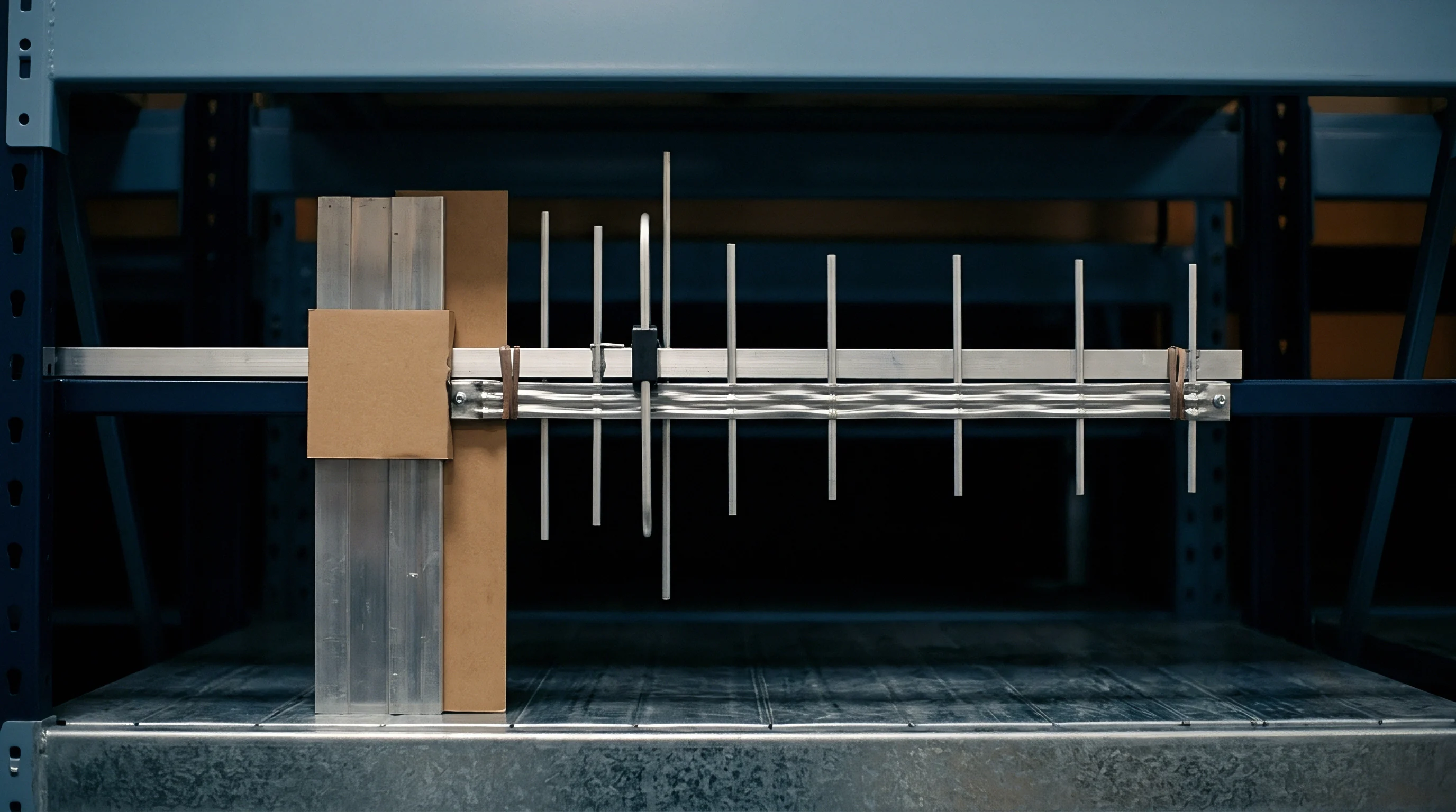
The fixture itself brings in measurement uncertainty. Brackets made of structural foams or lossy plastics generate secondary reflections that degrade phase accuracy during near-field planar scans. Calibration labs rely on low-density polystyrene holders with a relative permittivity below 1.05 to support both the device under test and the phantom slab.
Placing a metallic bracket within forty millimeters of the active face ruins the spatial power density integration, an error frequently blamed on mechanical misalignment rather than RF coupling from the test hardware.
Reconstruction
Spatial power density evaluation hinges on calculating energy transfer across a surface located just off the device housing. Regulators, including the Federal Communications Commission in the United States and member-state authorities across the European Union, mandate compliance with incident power density limits ~ typically twenty watts per square meter averaged over four square centimeters. Because mapping both electric and magnetic field vectors across dense grids at millimeter-wave frequencies runs into severe mechanical limits, labs rely on mathematical field transformations instead.

Can Mathematical Solvers Reconstruct Distorted Aperture Fields?
Equivalent source algorithms address this challenge by converting measured tangential near-field data into equivalent electric and magnetic surface currents. Scans recorded between two millimeters and ten millimeters from the housing provide the input boundary conditions. By inverting the radiation integral, the algorithm maps currents back to the array face, capturing local impedance shifts produced by nearby dielectric loading.
Phase retrieval routines avoid the requirement for vector receivers altogether: taking two separate amplitude-only planar scans at different heights above the array lets iterative solvers reconstruct the aperture phase profile directly.
A concrete example illustrates how spatial averaging behaves under severe loading. Take a four-by-four patch array running at twenty-eight gigahertz with element spacing of 5.35 millimeters, giving an aperture area of roughly 4.58 square centimeters. Radiating into free space at twenty decibel-milliwatts input (100 milliwatts), the array generates a peak spatial power density of eighteen watts per square meter at a distance of five millimeters.
Bringing an artificial hand phantom to within two millimeters pulls the active impedance off match, cutting total radiated power by 1.8 decibels down to 66 milliwatts while sidelobes climb unpredictably during beam steering.
Local field concentration completely changes the compliance picture. The dielectric slab refracts reactive energy into a smaller effective footprint, focusing a hot spot directly under the lower quadrant of the array. Peak un-averaged power density reaches thirty-eight watts per square meter across a circular spot of 0.8 square centimeters.
Averaged over the four-square-centimeter window defined by FCC Part 30 and Part 2.1093, the spatial density comes out to 22.4 watts per square meter. A design that clears limits in free space ends up exceeding the statutory cap by 12 percent once proximity loading focuses the near-field energy.
A twenty-decibel-milliwatt transmitter array passing free-space power density limits fails four-square-centimeter spatial compliance when dielectric refraction concentrates energy into localized near-field peaks.
Phase reconstruction hits practical limits once the measurement surface enters the reactive zone of the probe. Iterative retrieval routines struggle to converge when steep evanescent waves decay across intervals smaller than the robot’s positioning repeatability. At that threshold, test engineers are left trying to determine whether an apparent power density peak is a physical hot spot or an artifact generated by spatial sampling noise in the solver.


Deformation
Anechoic chamber radiation patterns rarely hold once a radio operates next to human tissue. Beam codebooks hardcoded into baseband firmware assume spherical propagation into isotropic space. Near-field loading reshapes the radiation envelope entirely, reducing peak equivalent isotropically radiated power, raising sidelobes, and pulling pointing vectors off their commanded targets.
Where Does near Field Power Density Compliance Fail?
Pattern degradation hits scan angles unevenly. Steering thirty degrees off-boresight sets up asymmetric active impedances across array rows: elements closest to tissue face heavy dielectric loading, while elements on the far side retain higher radiation efficiency. The resulting beam pulls toward the unloaded elements, producing an uncommanded pointing offset.
At steering angles beyond forty degrees, proximity loading frequently causes pointing errors between four and eight degrees.
| Array Geometry | Commanded Angle | Loading Condition | Peak EIRP Delta | Pointing Error | Compliance Status |
|---|---|---|---|---|---|
| 1×4 Dipole Module | 0 deg (Boresight) | Free Space Baseline | 0.0 dB | 0.0 deg | Compliant (12 W/m²) |
| 1×4 Dipole Module | 30 deg Azimuth | Palm Phantom (2 mm) | -3.8 dB | 4.2 deg | Compliant (17 W/m²) |
| 2×4 Patch Array | 0 deg (Boresight) | Head Phantom (5 mm) | -2.2 dB | 1.1 deg | Compliant (14 W/m²) |
| 2×4 Patch Array | 45 deg Azimuth | Hand Phantom (1 mm) | -5.6 dB | 7.8 deg | Non-Compliant (24 W/m²) |
| 4×4 Patch Matrix | 30 deg Elevation | Torso Phantom (10 mm) | -1.9 dB | 2.4 deg | Compliant (16 W/m²) |
Hardware integrators encounter regulatory exposure risks along specific deployment vectors:
- Side Lobe Regrowth elevates electromagnetic emissions in non-target directions, exceeding spurious emission masks or incident power density limits at unexpected angles.
- Main Lobe Broadening disperses directed energy across a wider spatial volume, lowering link margin below cellular communication standards.
- Polarization Ellipticity Drift converts nominal linear polarization into degraded elliptical polarization, increasing polarization mismatch losses at the distant receiver.
- Codebook Null Shifting moves pre-calculated pattern nulls away from internal victim receivers, degrading co-located sensor or radio receiver sensitivity.
The compliance risk is particularly sharp under European Union market access rules. Directive 2014/53/EU (the Radio Equipment Directive) requires technical files to prove conformity with Article 3.1a for health and safety alongside Article 3.2 for spectrum efficiency under realistic operating conditions. If proximity loading broadens the main beam or drives sidelobes past the boundary masks set in harmonized standard ETSI EN 301 908-25, self-declaration routes leave a manufacturer vulnerable to market surveillance actions, mandatory product recalls, and impounded shipments at EU ports of entry.

Recalibration
Managing proximity loading demands real-time hardware response rather than static calibration tables. Firmware must detect nearby obstacles and alter transmit parameters on the fly. Current millimeter-wave designs place dedicated capacitive or optical proximity sensors along chassis perimeters to register a user’s grip before the phased array transmits at full power.
Tripping a sensor prompts the modem to cut power or toggle to a secondary codebook tailored for loaded operation. Technical documentation for an FCC Part 30 filing has to describe this dynamic power reduction mechanism in detail, and test engineers must demonstrate that power backoff triggers consistently across different hand grips, temperature ranges, and skin conditions, since an unresponsive sensor fails the device on the spot.
Modular approvals rarely protect production schedules as much as integration teams expect. Sourcing pre-certified millimeter-wave radio modules looks like a shortcut, but the modular grant assumes an open environment that disappears behind custom enclosures, display assemblies, or metallic frame rails. Under FCC modular rules, altering the casing geometry, modifying sensor routing, or adding dielectric load over the antenna voids the existing grant, triggering either a Class II Permissive Change or a ground-up recertification filing.
A full millimeter-wave compliance campaign covering incident power density mapping and sensor verification takes eighty to one hundred twenty hours in an RF chamber, with accredited test facilities billing between six hundred and nine hundred dollars per hour. Retests compound those costs: when unexpected radome properties alter near-field coupling, debugging and codebook re-indexing can eat up six to ten weeks of engineering work and forty thousand to seventy thousand dollars in extra test fees while commercial launch windows slip away.
Host manufacturers mitigate schedule delays and customs holds by running near-field pre-compliance scans early in mechanical prototyping, testing active reflection coefficients against physical dielectric slabs before freezing housing resin specifications.