Meaning
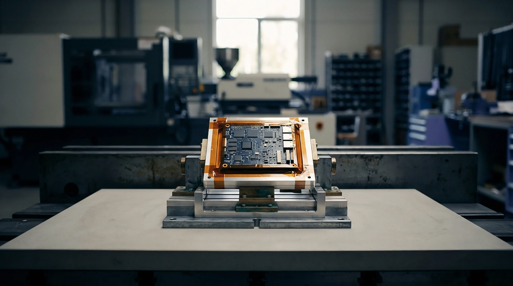
Electronic design automation software provides a unified environment for schematic capture and printed circuit board layout. Multi-layer routing and high-speed design rules are managed within altium designer to prepare production files for fabrication. This tool integrates mechanical constraints with electrical connectivity to ensure correct component placement.
Design Environment
Schematic sheets are linked to layout files to maintain netlist integrity. Designers use altium designer to specify track widths, layer stackups, and via transitions. High-speed signal paths are tuned to match lengths across parallel buses.
Output Generation
Manufacturing files are generated from the completed layout to guide assembly and board fabrication. Output directories in altium designer hold gerber files, drill schedules, and pick-and-place lists. These files represent the final physical pattern and hole locations of the board.
Assembly partners use this documentation to configure pick-and-place machinery. The generation of a bill of materials completes the release package, specifying manufacturer part numbers and package descriptions for procurement.
Integration Parameter
Mechanical CAD files are imported into the workspace to verify the fit of the board within a housing. In altium designer, three-dimensional models of components show collisions with enclosures or connectors. This validation reduces the need for multiple physical prototypes.