Meaning
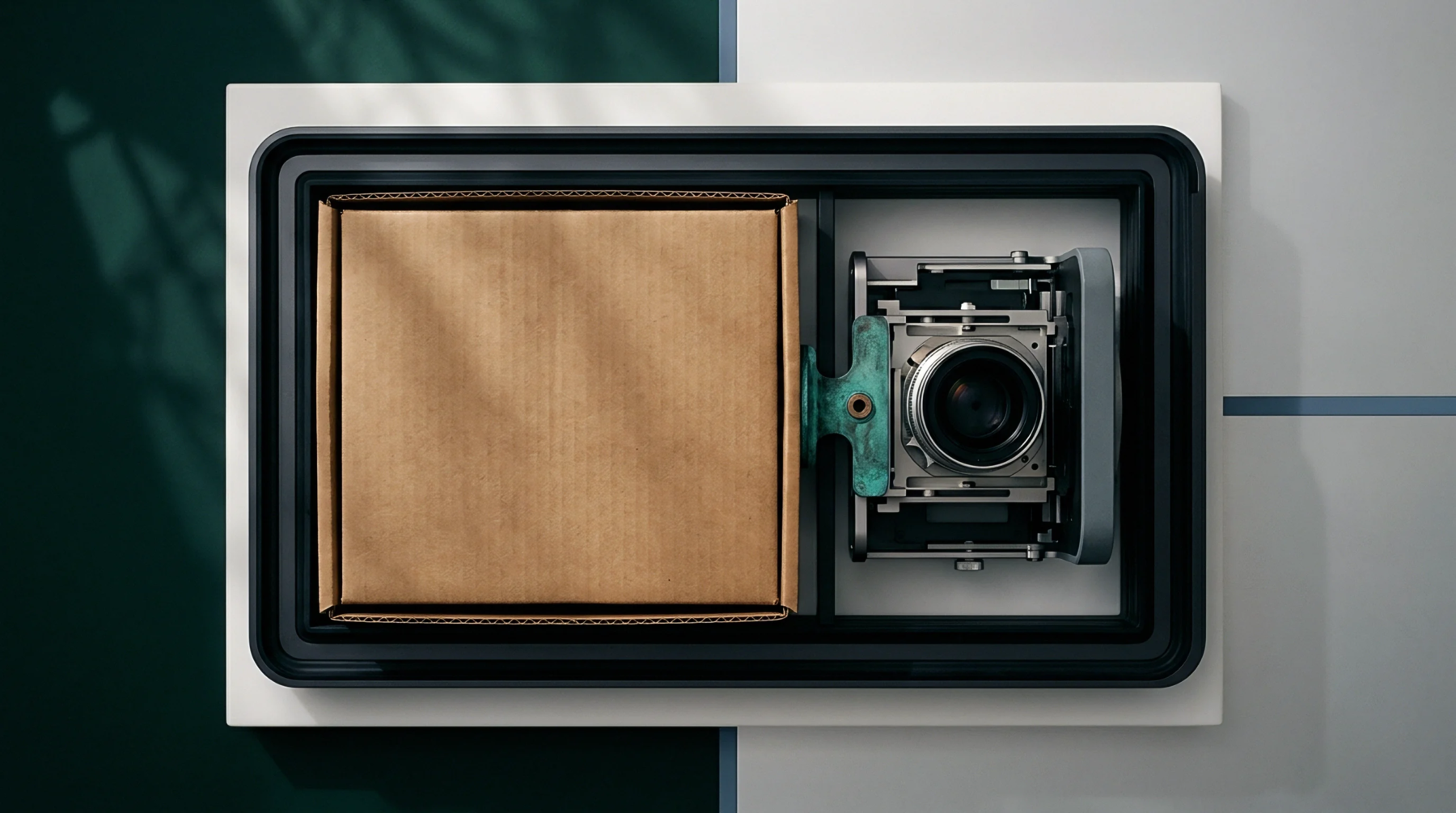
High-resolution imaging systems scan assembled printed circuit boards to identify manufacturing defects after component placement or reflow soldering. By utilising multi-angle cameras and programmed algorithms, automatic optical inspection detects missing components and board misalignments. The technology verifies the physical integrity of electronic assemblies before they proceed to functional testing.
Defect Detection
Surface mount components must align perfectly with their designated pads to prevent electrical failure or mechanical stress. Modern inspection algorithms compare the captured board image against a golden board or a CAD dataset to identify solder voids and polar deviations. This automated comparison prevents faulty boards from advancing in the assembly line, minimizing waste and rework costs.
High-magnification lenses allow the system to resolve sub-millimetre features on extremely dense layouts.
Inspection Throughput
Production velocity relies on fast scan rates to match the cycle time of high-speed placement machines. Placing the system directly after the reflow oven ensures rapid feedback. This positioning minimizes the volume of defective boards.
Process Integration
Integrating this automated system reduces the manual inspection burden and stabilizes production yield. Although it locates visible surface anomalies, it cannot evaluate internal solder structure or subsurface voids. Complementary technologies like X-ray imaging are necessary to inspect hidden solder joints.