Establishing Baseline Optical Sensor Calibration Standards for In-Line Assembly
Baseline optical calibration on assembly lines eliminates mechanical housing tolerances and cross-talk offsets through traceable in-fixture stimulus standards.
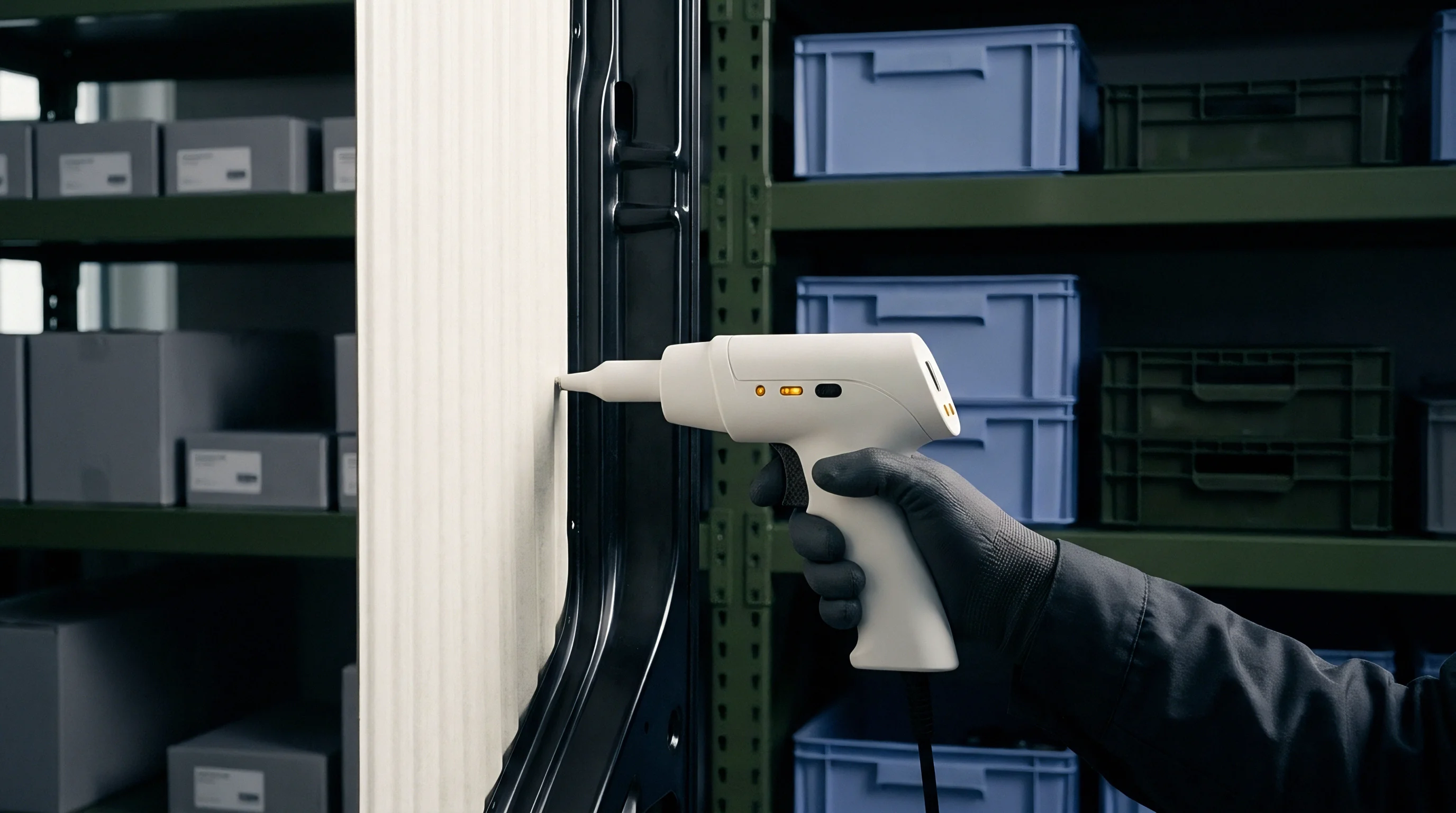
Beam
A bare surface-mount photodetector soldered to a four-layer carrier board delivers performance that quickly shifts once protective clear polycarbonates, structural housings, and high-volume placement variations enter the picture. Evaluation boards from silicon vendors mask this reality by using hand-selected, center-bin semiconductors mounted in open-air optical cavities. On an automated pick-and-place line, production units see angular tilts up to three degrees, solder reflow meniscus variations that alter planar height by fifty micrometers, and radiant sensitivity distributions spanning plus or minus twenty percent across a single wafer lot.
Engineering teams integrating optical transceivers, time-of-flight rangefinders, or ambient light sensors into enclosures often try to bypass factory calibration by locking firmware registers to the typical values on page six of a component datasheet. But silicon vendors calibrate those baseline numbers using an idealized lambertian source perpendicular to the die at a steady junction temperature of twenty-five degrees Celsius. Real production lines operate under shifting ambient light, factory temperatures swinging between eighteen and thirty-four degrees Celsius, and localized thermal gradients from downstream selective soldering equipment.
Optical sensor baseline calibration fixes electrical gain against mechanical assembly tolerance rather than confirming nominal silicon datasheet performance.
When an optical emitter like a vertical-cavity surface-emitting laser or a narrow-band infrared light-emitting diode sits alongside a photodiode array behind a shared cover, internal reflections dominate the initial signal. Structural adhesives, gasket compression tolerances, and residual stress around resin mold gates create optical cross-talk that shows up as a false target or an elevated dark-current floor. A baseline calibration standard establishes the reference operating point that downstream algorithms need to calculate actual target displacement or optical density.
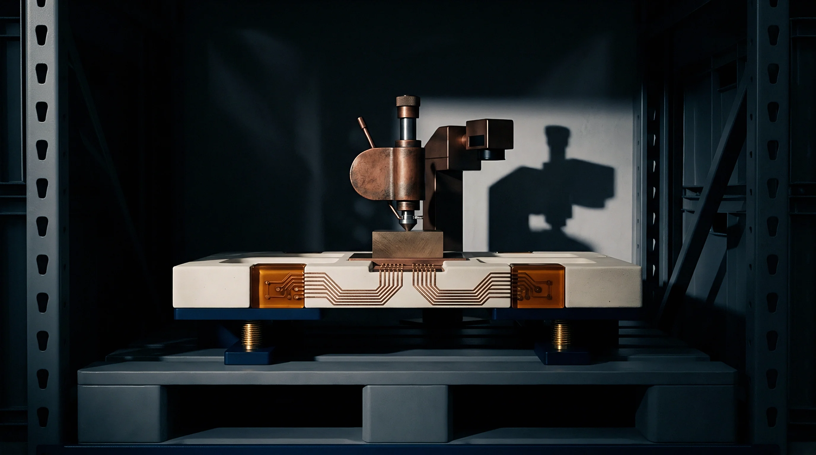
Optical Register Presets versus Dynamic Characterization
Integrated ambient light and proximity modules package the sensing element, transimpedance amplifier, analog-to-digital converter, and internal clock onto a single system-on-chip. Reference firmware from semiconductor vendors writes default settings to the sensor’s internal registers over I2C or SPI at power-on reset. These presets set integration time, analog gain multipliers, and emitter drive current, but they assume idealized transmission through ninety-two percent transparent optical glass.
In practice, protective covers cut optical transmission down to thirty or forty percent in visible spectra just to hide internal electronics, while introducing spectral attenuation slopes that throw off color ratios. Solder flux outgassing during reflow leaves microscopic residue on sensor apertures, pulling down baseline responsivity before the housing is even closed. Factory calibration writes specific baseline offset values into non-volatile memory or on-chip one-time-programmable bits to cancel out ambient noise and reflections from the housing.
Mechanical Tolerances Shifting Optical Alignment
High-speed placement machines inevitably introduce rotational and translational offsets. A photodiode with an active area measuring five hundred micrometers across suffers a noticeable loss in optical throughput if an aperture plate shifts two hundred micrometers off center. That geometric misalignment skews the effective field of view, turning what should be a wide-angle response into an asymmetric reception cone.
The interplay between emitter cone divergence and receiver acceptance angle determines the baseline signal floor. If an assembly seats the sensor deeper inside an enclosure recess, side-wall clipping cuts secondary lobe light while scattering secondary reflections back into the sensor. In-line calibration measures this parasitic baseline directly, saving a zero-point compensation coefficient in system flash memory so the internal analog front end does not saturate early.
Factory calibration can appear redundant when modern sensing silicon incorporates internal temperature compensation loops and automated dark-current cancellation routines.

Lamp
Physical calibration standards on automated production lines depend entirely on the optical stability and spectral distribution of the stimulus fixture. Integrating spheres lined with sintered polytetrafluoroethylene produce uniform radiance across test ports, but the light sources driving them degrade over continuous production cycles. Halogen baseline lamps suffer filament evaporation that drags color temperature downward over hundreds of operating hours, while solid-state narrow-band emitters experience junction degradation, power drop, and spectral center-wavelength drift.
An in-line optical calibration station shields the sensor assembly from ambient factory light using pneumatically actuated hoods lined with optical absorbing polyurethane foam. Stray light leaking past cable feedthroughs or pneumatic conduits creates offset errors that ruin baseline zero-point calculations. The fixture checks dark-current levels before firing active light sources, aborting the cycle if ambient leakage exceeds one-tenth of the least significant bit of the sensor’s internal analog-to-digital converter.
| Source Architecture | Spectral Bandwidth (nm) | Short-Term Drift (8h) | Annual Degradation Rate | Recalibration Interval |
|---|---|---|---|---|
| Tungsten-Halogen Regulated Lamp | 380 to 2500 | 0.8 percent | 5.0 to 8.0 percent | 500 operating hours |
| Narrow-Band Surface Mount LED | 15 to 35 | 1.2 percent | 3.0 to 6.0 percent | 1000 operating hours |
| Temperature-Stabilized VCSEL Array | 0.8 to 2.0 | 0.3 percent | 1.5 to 3.0 percent | 2000 operating hours |
| Plasma Discharge High-Intensity Source | 200 to 1100 | 2.1 percent | 9.0 to 14.0 percent | 250 operating hours |

What Establishes Traceability across Factory Tiers?
Calibration integrity relies on an unbroken traceable chain from the factory test jig back to national metrology standards maintained by the National Institute of Standards and Technology or equivalent international bodies. A working photometer or master reference sensor mounted inside the production fixture monitors delivered irradiance continuously, and is periodically cross-checked against a transfer standard based on cumulative exposure hours.
Factory floors bring vibration, thermal swings, and dust that degrade reference fixtures far faster than controlled lab environments. Dust settling on an integrating sphere’s entry ports cuts radiant flux, artificially lowering measured sensor responsivity. Automated monitoring loops compare reference sensor output against drive-current thresholds, triggering a maintenance alert whenever source output strays from baseline tracking curves.
Standard practice requires transfer calibration standards to maintain at least four times the accuracy margin of the sensor unit under test.
Master golden units from early pilot runs provide a practical check on the assembly line. Line operators load these units at the start of each shift to verify fixture repeatability. If a golden unit suffers electrostatic damage or mechanical impact, it can skew the entire shift toward false failures or systematic offset errors.
Because golden units age and accumulate haze on optical surfaces, they need scheduled replacement with secondary masters kept in controlled storage.

Fixture Geometry and Spatial Uniformity Constraints
Spatial non-uniformity across the fixture’s illumination field translates straight into gain error. A device sitting two millimeters off-axis inside a low-cost collimator receives fifteen percent less optical flux than a centered unit, causing the calibration script to over-compensate analog gain. Nesting mechanisms must align the sensor package with repeatable kinematic clamping that prevents tilt and lateral movement at production speeds.
- Kinematic nesting pins align the printed circuit board assembly along primary datum edges to keep lateral positioning variance under twenty-five micrometers across all axes.
- Pneumatic clamping heads apply balanced downward force to non-optical areas of the substrate, preventing board flexure during exposure.
- Internal reference monitor channels sample peripheral flux inside the delivery tube during exposure to normalize source voltage ripple in real time.
- Baffled absorption baffles eliminate secondary grazing reflections between the test fixture exit pupil and the outer surface of the device enclosure.
A reference source drifted out of alignment produces flawless test logs that mask dead devices.

Variance
Optical response curves shift non-linearly over temperature. Silicon photodiode responsivity has a positive temperature coefficient in the near-infrared spectrum, rising roughly two-tenths of a percent per degree Celsius as the bandgap narrows. If a calibration station measures baseline sensitivity while the package is still warm at thirty-five degrees Celsius after functional testing, board units calibrated after a cold twenty-degree shift restart will fail low-light threshold checks.
Assembly lines cannot pause for long thermal soak cycles to bring every board to exact equilibrium. Instead, the test routine reads die temperature from the sensor’s built-in thermal diode, applying an algorithmic offset to normalize the baseline back to twenty-five degrees Celsius. Calibration software that skips this step can introduce up to twenty percent seasonal variance between winter and summer production runs.
Can Short Integration Cycles Preserve Dynamic Range?
Tight cycle times force calibration routines into narrow timing windows. Optical sensors face classic trade-offs between analog integration time, noise floor, and baseline resolution. Longer integration times reduce quantization noise and make it easier to detect low-level parasitic reflections, whereas short integration windows introduce Poisson shot noise and digitizer jitter that degrade offset calculations.
Take a proximity module calibration targeting a baseline dark-current offset resolution of twelve bits. The transimpedance amplifier needs time to settle after gain switches so transient ringing does not corrupt initial samples. Skipping that delay shaves three seconds off cycle time, but it dumps high-frequency power rail noise straight into the baseline register.
| Integration Window (ms) | Station Takt Time (s) | Signal-to-Noise Ratio (dB) | Offset Uncertainty (LSB) | Throughput (Units/Hour) |
|---|---|---|---|---|
| 10 | 1.8 | 38.2 | plus or minus 14 | 2000 |
| 50 | 2.4 | 46.5 | plus or minus 5 | 1500 |
| 100 | 3.2 | 52.1 | plus or minus 2 | 1125 |
| 400 | 5.8 | 64.8 | plus or minus 0.5 | 620 |
Thermal stress during surface-mount reflow shifts optical filter bandpass profiles. As package mold resin cools, mechanical stress acts on dielectric interference coatings deposited on the optics. This moves center-wavelength passbands by several nanometers, clipping signal transmission when paired with narrow-band emitters.
Calibration performed before final assembly misses these post-reflow shifts entirely, which is why baseline verification must happen on fully consolidated assemblies.
Baseline calibration sets performance boundaries for the life of the product. Optical components degrade with age: vertical-cavity lasers can drop twenty percent of their output power over five years, while photodiode dark currents rise as crystal defects migrate under electrical stress. A baseline calibration that consumes all available analog gain during assembly leaves no margin for automatic gain control to adjust later in the field.
A baseline calibration that consumes more than sixty percent of available analog front end compensation range produces field failures once environmental grime accumulates.
Calculating the optical link budget requires accounting for every baseline tolerance stack-up. Consider an ambient sensor assembly where a nominal, unattenuated target produces a two-volt swing at the transimpedance amplifier output. Internal optical cross-talk from the housing contributes a four hundred millivolt offset under normal conditions.
If component tilt adds one hundred millivolts, window haze adds fifty millivolts, and fixture light leakage adds another fifty millivolts, total parasitic baseline voltage reaches six hundred millivolts ~ eating thirty percent of the available dynamic range before any target is detected.
Underestimating baseline variance risks field recalls when devices permanently saturate and lock up under direct sunlight.

Custody
The gap between a contract manufacturer and an original equipment manufacturer shows up most clearly around calibration data ownership and fixture maintenance. Turnkey manufacturing quotes usually fold functional testing into a general line fee, obscuring the cost of optical sources, traceability audits, and cycle-time overhead. When yields drop, arguments follow over whether the root cause lies in silicon tolerances, optical housing quality, or fixture drift.
Original equipment manufacturers need to state clearly who designs, owns, and programs the calibration software. Test routines running on assembly stations interact directly with sensor registers, burning calibration factors into non-volatile memory or saving look-up tables in system storage. If a manufacturer controls that test sequence without providing source code, the buyer cannot move production to another facility without rebuilding the calibration system from scratch.

Allocation of Tooling and Non-Recurring Engineering
Building an optical calibration station requires dedicated non-recurring engineering for optomechanical fixtures, integrating spheres, transfer standards, and automation drivers. Manufacturing agreements should break these expenses into clear asset registers. Fixtures paid for under custom engineering charges legally belong to the buyer, along with schematics, scripts, and source code, preventing vendor lock-in if production moves.
- Optical fixture CAD drawings detail mechanical nesting clearances, aperture baffle dimensions, and pneumatic clamping footprints so duplicate tooling matches initial station performance.
- Automated test execution scripts include compiled binaries and raw source code connecting test hardware to the target board, ensuring portability across platforms.
- Traceability calibration logs record raw sensor counts, stimulus levels, ambient temperature, and calculated offset registers for every serialized unit leaving the line.
- Master sensor verification procedures define handling limits, maximum operating hours, and lab recalibration workflows for all golden reference devices.
Scrap allowances on the factory floor often mask calibration issues. Contract manufacturers routinely classify failed units as component defects, claiming credit from silicon vendors or passing costs back to the customer. In reality, unshielded test fixtures or unstable light sources cause false failures that drop yields and inflate assembly costs under the guise of scrap.
Design Transfer Package Requirements for Calibration
A thorough design transfer package sets clear repeatability rules across different manufacturing sites. Baseline calibration limits need statistical definitions rather than single fixed numbers. Documentation must specify upper and lower control limits for optical offsets, allowable gain adjustment ranges, and minimum correlation coefficients relative to reference standards.
Production audits verify whether factories execute calibration maintenance on schedule. Lamp hour tracking, integrating sphere cleanliness checks, and dark-chamber leak tests belong in secured electronic logs rather than on paper clipboards. Without verifiable maintenance checks, calibration stations drift, passing out-of-spec boards that fail environmental testing later on.
Section 14.2 of standard electronics manufacturing service agreements stipulates that all tooling, fixtures, test software, and calibration records paid via non-recurring engineering charges remain the exclusive property of the buyer and must be surrendered within fifteen business days of formal written transfer notice.