Meaning
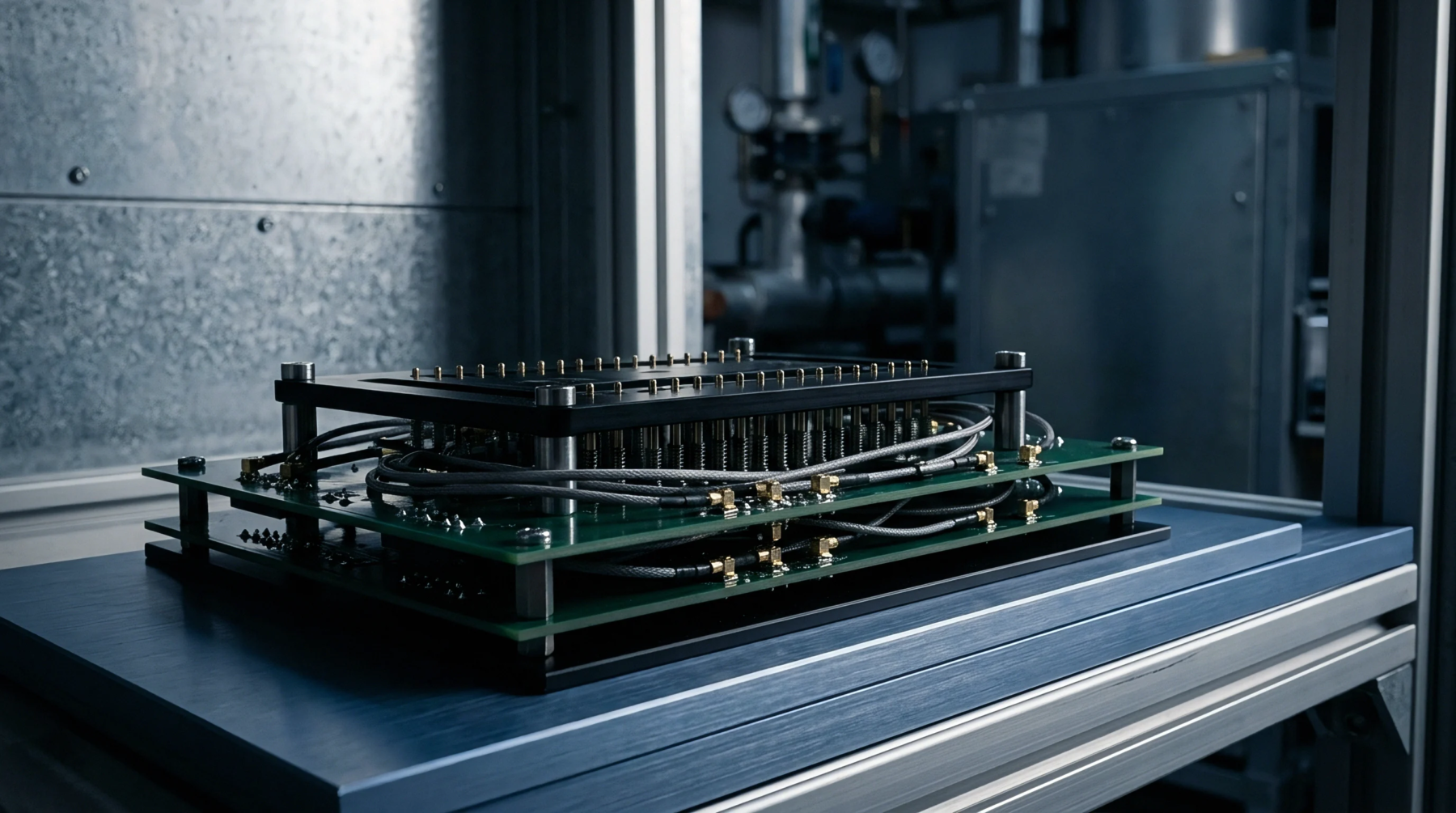
Electrical testing of printed circuit boards without using dedicated test pads improves routing density on complex multilayer assemblies. By omitting traditional test points, padless board testing utilizes vias and existing component pads to establish electrical contact. This approach minimizes parasitic capacitance and signal distortion in high-frequency circuits.
Physical Accessibility
Accessing tiny circuit nodes requires high-precision flying probe systems capable of sub-mil registration accuracy. Traditional test fixtures are unable to target these fine-pitch features reliably. High-density designs employ this strategy to recover valuable board real estate for signal routing and power distribution.
Probe Integration
Coordination between the electrical CAD layout and the flying probe programming is necessary to run these non-destructive checks. Flying probe equipment positions micro-needles on vias or component leads using advanced vision alignment systems. Laser correction corrects for board warping and manufacturing tolerances during the test cycle.
This automation assures that delicate contact areas remain undamaged by the test probes.
Manufacturing Advantage
Reduction in board area directly lowers the fabrication costs of high-density interconnect designs. Eliminating thousands of test pads simplifies the layout phase and shortens the design cycle. It also prevents signal degradation caused by the stub effects of long test trace routes.