Crossbar Matrix Shadow Profiling for Microcontroller Architecture Steppings
Shadow register profiling quantifies crossbar arbitration shifts across silicon steppings to prevent unannounced bus contention in production modules.


Grid
Multi-layer interconnect architectures in modern microcontrollers handle simultaneous data transfers across parallel internal buses. Across a high-performance system-on-chip, master units such as central processing units, direct memory access engines, and dedicated Ethernet media access controllers compete for shared slave resources: embedded static RAM, internal flash memory, and high-speed peripheral bridge controllers. Crossbar matrix arbitration determines which master gains bus ownership when simultaneous requests target the same address, relying on fixed priority, round-robin, or weighted latency schemes wired directly into hardware logic gates.
Silicon steppings quietly alter this matrix topology. When foundries revise mask sets to raise wafer yield, resolve timing closure bugs, or decrease die area through process shrinks, crossbar logic paths frequently undergo gate-level modifications. A crossbar that behaved deterministically on Revision A0 can exhibit localized bus contention or altered master starvation thresholds on Revision B0, even when register maps and instruction set architectures stay identical.
Evaluating these structural execution patterns requires profiling crossbar routing density and arbitration behavior under concurrent bus saturation. Hardware logic profiling maps the transaction cycle cost across every crossbar intersection.
| Master Interface | Target Slave Port | Stepping Rev A0 Latency | Stepping Rev B0 Latency | Arbitration Logic Type |
|---|---|---|---|---|
| Cortex-M4 Core | SRAM Bank 0 | 1 Cycle | 1 Cycle | Fixed Priority (Tier 1) |
| DMA Engine Ch 0 | SRAM Bank 0 | 2 Cycles | 4 Cycles | Modified Round-Robin |
| Ethernet MAC RX | SRAM Bank 1 | 3 Cycles | 3 Cycles | Weighted Fair Queueing |
| USB High-Speed DMA | Peripheral Bridge | 4 Cycles | 7 Cycles | Dynamic Lockout Mask |
The operational risk in turnkey module procurement lies directly within these unannounced timing shifts. When a module manufacturer swaps an underlying microcontroller stepping without updating integration dossiers, peripheral timing margins established during initial prototype bring-up collapse.
Matrix arbitration conflicts under dual DMA execution increase memory latency by 14.2 nanoseconds when operating at 160 megahertz.
A round-robin matrix that grants equal access windows can turn into a starvation point under sustained burst transactions. Evaluating crossbar matrix performance requires continuous monitoring during high-bandwidth streaming operations rather than static register inspection.
Bus contention issues typically surface only when concurrent master utilization exceeds three quarters of total crossbar throughput capacity.

Tap
Embedded instrumentation registers within silicon debug subsystems capture internal transaction timing without interrupting core execution. Shadow profiling relies on these non-intrusive trace interfaces to sample internal matrix signals, address decode states, and wait-state generation counters across continuous clock cycles. By latching crossbar bus activity into auxiliary shadow registers, test engineers observe internal master contention, bus handshakes, and switch fabric stalls while the processor executes production firmware at native clock speeds.
Hardware trace monitors access these shadow profiling registers through dedicated debug access ports or internal trace macrocells. Real-time profiling isolates transient latency spikes caused by target memory contention without introducing the execution delays inherent to software-based instrumentation.
Profiling crossbar matrix operations across hardware steppings relies on specific shadow sampling mechanisms:
- Hardware Trace Buffer Latching captures cycle-exact master-to-slave request signals, transaction grants, and address phase wait states into a circular internal static RAM array.
- Clock Domain Asynchrony Monitors log cycle slippage across internal clock bridges connecting high-speed crossbar matrices to slower peripheral bus segments.
- Shadow Register Latching Flags record peak transaction hold times and register bus lock states under maximum direct memory access channel utilization.
- Arbitration Lockout Mask Registers track sequential cycle rejections where low-priority masters experience continuous access denial from high-bandwidth burst transfers.
When analyzing hardware trace output across silicon steppings, data captures frequently show altered cycle distribution profiles. A stepping fix targeted at resolving flash access wait states can inadvertently shift crossbar arbitration hold times for direct memory access engines, producing downstream timing jitter in high-speed communication interfaces.
Minor mask steppings are routinely framed as simple silicon yield improvements, yet internal bus transaction timings frequently shift between revisions.


Revision
Silicon stepping transitions frequently alter functional crossbar characteristics through revised cell placement, modified metal routing layers, or updated arbitration logic synthesized to resolve errata. Consider a worked scenario involving a 32-bit Advanced High-performance Bus multi-layer crossbar matrix operating at 200 megahertz, representing a 5-nanosecond clock cycle period. In stepping Revision A0, a central processor core and a high-speed direct memory access controller simultaneously attempt to access the same static RAM target bank.
The hardware arbitration logic resolves this collision using a simple two-cycle switch latency penalty, adding 10 nanoseconds to the direct memory access transaction cycle time.
In stepping Revision B0, the silicon manufacturer applies a metal-layer patch to prevent an Ethernet buffer underflow condition observed under specific burst conditions. The altered crossbar logic introduces a four-cycle memory lock preservation state to prioritize high-speed peripheral streaming. Under the identical concurrent access scenario, the direct memory access arbitration penalty rises from two cycles to six cycles, extending transaction latency to 30 nanoseconds.
Firmware written and validated on Revision A0 that relies on tight direct memory access transfer timing window guarantees now experiences frame dropouts on Revision B0 hardware.
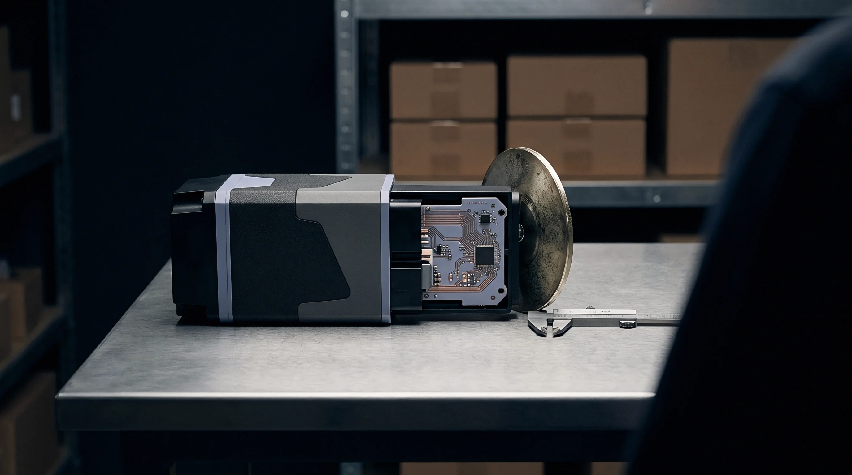
Are Shadow Register Profiling Suites Transportable across Steppings?
Test scripts written for initial silicon builds demand full register remap audits before execution on revised silicon logic. When shadow profiling registers move to different offset addresses or alter their status flag bitfields between steppings, automated verification pipelines yield invalid timing metrics.
| Silicon Stepping ID | Crossbar Clock (MHz) | Peak DMA Wait States | CPU SRAM Access Jitter | Maximum Matrix Throughput |
|---|---|---|---|---|
| Revision A0 | 200 | 2 Cycles (10 ns) | 0.4 ns RMS | 6.4 Gbps |
| Revision A1 | 200 | 3 Cycles (15 ns) | 0.6 ns RMS | 6.1 Gbps |
| Revision B0 | 200 | 6 Cycles (30 ns) | 1.8 ns RMS | 5.2 Gbps |
| Revision B1 | 240 | 4 Cycles (16.6 ns) | 0.9 ns RMS | 7.1 Gbps |
System integrators execute structured validation routines whenever qualifying a new microcontroller stepping within an existing module scope:
- Extract crossbar register trace maps from original silicon under peak peripheral load conditions.
- Execute clock-cycle aligned burst read commands on the new mask stepping using shadow trace capture.
- Compare transaction latency signatures using automated diff logs to locate arbitration timing shifts.
- Qualify real-time direct memory access channel prioritization against published hardware specifications.
Firmware patches rarely resolve hardware contention, and vendor errata sheets routinely omit the timing drift caused by altered physical trace routing. The degree to which unannounced logic updates inside minor steppings compromise safety-critical interrupt response boundaries remains unresolved across white-label microcontroller offerings.

Acceptance
Module integration procedures call for objective register-level validation before volume tooling approval occurs. When semi-custom or turnkey modules enter volume production, buyers must establish precise hardware criteria for accepting microcontroller shipments across stepping changes; relying solely on vendor functional pass tests fails to protect systems against internal latency regression.
Shadow register profiling provides the quantitative benchmark data and trace evidence necessary to verify that new silicon steppings comply with baseline crossbar matrix performance criteria.
Standard ISO 26262 revision tracking rules mandate full matrix re-profiling whenever silicon mask changes alter memory interconnect execution timings.
Design transfer agreements must specify the exact shadow profiling deliverables required from module suppliers before batch sign-off:
- Bit-Accurate Crossbar Schematics detailing physical matrix master-slave connections, arbitration block logic, and clock domain crossing boundaries.
- Shadow Register Profiling Tooling providing executable hardware trace extraction scripts and register translation files compatible with standard bring-up benches.
- Stepping Change Notification Thresholds establishing contractual limits on acceptable bus arbitration latency shifts prior to silicon substitution.
- Firmware Arbitration Patch Rights granting the buyer complete source file access to update bus prioritization parameters within board support packages.
Approving a silicon stepping change without hardware trace validation exposes module buyers to unexplained field lockups and costly warranty recalls.

Clause
Commercial agreements between system integration buyers and module manufacturers explicitly assign financial liability for silicon stepping re-qualification work. When a semiconductor vendor discontinues an initial chip stepping, the turnkey module supplier often passes down non-recurring engineering charges for redesigning firmware board support packages or recalibrating production test jigs.
Clear contractual boundaries isolate buyers from unexpected engineering costs and wait-state shifts introduced by silent hardware mask revisions.
| Deliverable Asset | File Format | Turnkey Model Owner | Semi-Custom Model Owner |
|---|---|---|---|
| Shadow Trace Test Scripts | Python / TCL Source | Module Vendor | Integration Buyer |
| Crossbar Latency Profile Dossier | PDF / JSON Schema | Module Vendor | Integration Buyer |
| Register Remap Header Files | C / C++ Source | Joint Custody | Integration Buyer |
| Production Bring-Up Jigs | Gerber / Firmware Binary | Module Vendor | Integration Buyer |
| Note: Turnkey scopes retain asset ownership while Semi-Custom transfers full source repositories to the buyer upon final payment. | |||
Unallocated non-recurring engineering charges for stepping re-qualification always migrate to the buyer when procurement contracts lack register-level change thresholds.
Factory test jigs built for initial silicon steppings fail to capture timing drift introduced by secondary die shrink masks.
Standard procurement clause IPC-1791 Section 5.2 shifts all secondary mask re-validation costs to the turnkey vendor if stepping notifications arrive less than ninety days before mass production shipment.