Identifying Shared ODM Hardware Architectures across Competing Brands
Shared ODM architectures are identified through identical PCB layouts, matching device tree memory maps, unified tooling marks, and shared FCC test filings.
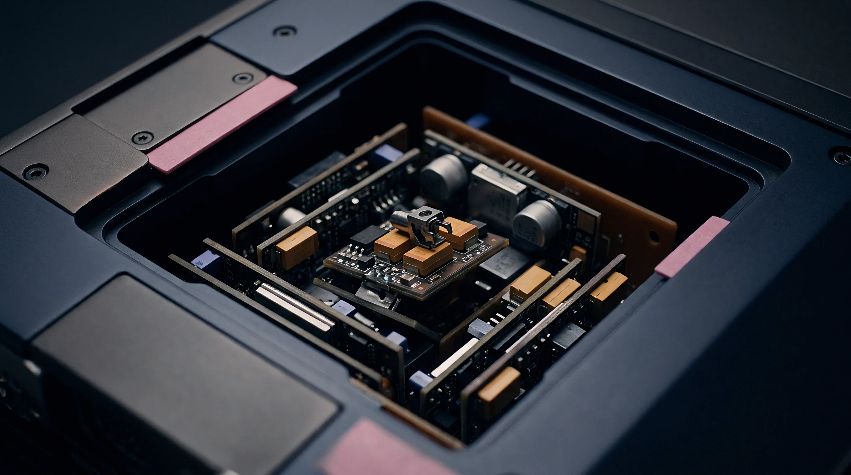

Anatomy
Silicon Identifiers and Substrate Clues
Original design manufacturers rely on unified base platforms to spread design validation testing and non-recurring engineering costs across multiple clients, leaving clear physical traces on the boards themselves. Opening competing chassis side-by-side often exposes identical silk-screen reference designators, showing that both brands pulled their layout from the exact same factory board spinning.
Silicon markings give away shared provenance almost immediately. Package labels on systems-on-chip, power management ICs, and discrete front-end RF modules routinely match across what are marketed as competing bills of materials. Chip vendors supply turnkey reference schematics directly to tier-one factories; when two competing enterprise access points or smart energy monitors share a wireless transceiver layout and an identical buck converter topology, they came out of the same facility.
Board stack-ups tell a similar story. Assembly plants stick to standard fabrication recipes to simplify panelization on surface mount lines, which means board thickness, dielectric constant tolerances, and ground plane cutouts line up across separate commercial brands.
Copper layer thickness variations inside high-frequency printed circuit boards rarely deviate past five percent between boards processed on the identical factory panel press.
Pick-and-place coordinate files show up clearly in component placement geometry. Even when retail products sport distinct outer plastics, badge designs, or secondary heat sinks, core components stay pinned to identical coordinates on the raw substrate. Measuring transceiver position relative to the reference crystal oscillator reveals matching PCB traces, with decoupling capacitors, passive clusters, and test point arrays taken straight from the same fab run coordinate export.

Teardown

Mechanical Interlocking and Fastener Schemes
Injection tooling is expensive, so shared platforms frequently reuse internal structural plastics while swapping out only the outer cosmetic shell. Screw bosses, snap latches, and internal stiffening ribs line up exactly between competing products sharing a factory base. Die witness marks, circular ejector pin impressions, and resin identification stamps all point back to the same mold tooling.
Thermal management follows suit. Sister products share die-cast aluminum RF shields, cold rolled steel heat spreaders, and identical phase-change thermal pad thicknesses. Heat sink fin counts, internal ducting, and spring-screw tension profiles match across brands.
A company reskinning an ODM reference board into a sleeker enclosure almost always keeps the internal metal framing untouched.
Internal wiring and connectors also reflect plant assembly habits. Ribbon cable pitch, board-to-board mezzanine heights, and routing paths for miniature coaxial cables show direct process reuse, drawn from common vendor catalogs that the factory uses across concurrent customer builds.
Which Clues Expose Shared Tooling Early?
Public regulatory filings offer a fast way to verify common origins without tearing down physical units. FCC test reports, CE technical construction files, and safety certifications require internal chassis photographs and RF compliance records, letting procurement teams spot shared hardware well before retail units ship.
Regulatory dossiers routinely expose identical platform hardware:
- Antenna pattern profiles document identical peak gain distributions and matching omnidirectional trace geometries inside otherwise distinct device enclosures.
- Radio frequency test data confirms identical harmonic suppression circuits, with matching spurious emission peaks and operating limits recorded on separate test dates.
- Schematic fragments in authorization filings reveal identical component designators, matching bus pull-up resistors, and duplicate power distribution rails.
- Printed circuit board revisions show internal factory alphanumeric codes etched directly into top-layer copper under the same revision numbering scheme.
Catching these factory signatures early gives buyers leverage during commercial negotiations, especially when an ostensibly bespoke proposal relies on an off-the-shelf ODM platform available elsewhere at volume pricing.


Firmware

Boot Sequences and Memory Partitions
Serial debug ports provide direct insight into underlying software. Tapping board-level UART pads or unpopulated four-pin headers exposes bootloader diagnostics as soon as power is applied, showing the silicon vendor, specific bootloader build branches, partition tables, and peripheral initialization routines.
| Hardware Diagnostic Plane | Factory Reference Platform | Turnkey Brand Variant | Semi-Custom Brand Variant |
|---|---|---|---|
| Bootloader String | Vendor U-Boot standard build | Stripped prompt with stock banner | Vendor U-Boot with branded build tag |
| Partition Table Map | Standard Flash 16MB allocation | Factory reference offset layout | Re-allocated user data partitions |
| I2C Bus Address Map | Stock PMIC, RTC, and sensor lines | Identical bus enumeration table | Identical base bus with added sensor |
| Device Tree Structure | Silicon vendor evaluation dts | Unmodified ODM base dts file | Minor GPIO remapping in peripheral nodes |
| MAC Address OUI Block | Silicon or ODM registered vendor | ODM registered company block | Brand registered corporate OUI |
Device trees define how the Linux kernel talks to board hardware. Decompiling the device tree blob extracted from boot media yields a full map of the board: pin multiplexing assignments, interrupt routings, and clock tree layouts match across products sharing an ODM platform. Even after a customer brand skins the user interface, underlying hardware nodes remain direct copies of the factory baseline.
Non-volatile flash partitions often follow the original factory template without modification. Dumping an SPI flash chip reveals matching byte offsets for bootloaders, kernel partitions, root file systems, and configuration blocks across different commercial devices. Factory recovery routines and legacy shell scripts frequently survive untouched in shipping production builds.
A compiled Linux device tree blob reveals base hardware identity through GPIO interrupt assignment tables that retain factory default pin names across competing consumer products.
Key management also exposes white-label production lines. Secure boot roots, authority certificates, and diagnostic keys often carry signatures from shared test certs. When factories fail to provision unique cryptographic keys for individual client runs, hardware from competing brands can end up responding to the exact same diagnostic unlock commands.


Ledger

Cost Structures and Engineering Allocation
Using an existing ODM hardware platform reshapes project economics. Turnkey designs bypass the non-recurring engineering fees required for ground-up multilayer PCB routing and RF compliance testing, but in exchange the buyer accepts fixed unit margins while surrendering rights to the raw schematics, production Gerber files, and factory test fixtures.
Non-recurring engineering costs scale with the degree of customization. A pure turnkey project incurs no board layout fees, requiring only order commitments and minor tooling costs for badging. Semi-custom designs run between 45,000 and 180,000 USD in NRE to cover modified enclosures, custom connector headers, and environmental qualification.
Fully bespoke hardware pushes development budgets past 400,000 USD once ground-up layout, hard tooling, international radio approvals, and production line setup are factored in.
Unit pricing mirrors these ownership dynamics. An ODM amortizing development across five separate retail clients leverages pooled volume to negotiate cheaper component pricing from silicon vendors. The brand gets lower unit costs on early low-volume runs, but finds itself locked into that single supplier when scaling up and unable to move manufacturing elsewhere.
Design ownership is where hardware buyers take on the most commercial risk. On semi-custom projects, the ODM typically maintains full control over foundational files:
- The buyer executes an initial development agreement with vague source code and schematic transfer milestones.
- The ODM delivers compiled binary images, basic functional test reports, and outward dimension drawings while withholding native Altium, Cadence, or Gerber X2 production manufacturing packages.
- Production volume scales to intermediate commercial levels where unit margins become financially restrictive for the brand.
- The brand issues a design transfer request to qualify a secondary manufacturing partner in an alternate geographic region.
- The original ODM asserts absolute ownership over the base platform circuit layout, refusing to release bill of materials supply chain sources or factory test fixture specifications without prohibitive intellectual property buy-out fees.
Contract clauses assigning base platform rights to the designer prevent production moves, keeping the buyer tied to that factory until the product reaches end of life.


Discrepancy

Variance Modeling in Shared Silicon Platforms
Small hardware variations regularly appear across products sharing the same core platform. Manufacturers adjust passive components, swap peripheral sensors, and tweak heat sinks to match different brand price tiers. Isolating these differences separates cosmetic changes from the underlying reference platform.
Power delivery circuits are a frequent target for unpopulated parts. A premium brand variant might run a four-phase buck regulator populated with solid polymer capacitors for heat tolerance, while a cheaper sibling on the same board drops to three phases with standard electrolytic cans, leaving bare solder pads on the substrate. The copper routing and silk-screen markings remain identical on both.
| Architecture Modification Category | Design Change Scope | Typical NRE Cost Range (USD) | Time to Production (Weeks) | Transfer Feasibility |
|---|---|---|---|---|
| Cosmetic Shell Modification | Tooling inserts and exterior texture | 12,000 to 35,000 | 4 to 8 | Complete tooling custody retention |
| Component De-population | BOM changes without PCB re-spin | 3,000 to 8,000 | 2 to 4 | Tied to original factory SMT setup |
| Peripheral I/O Expansion | Daughterboard addition via header | 15,000 to 45,000 | 6 to 12 | Daughterboard portable; base locked |
| RF Layout Tuning | Passive matching network shift | 8,000 to 20,000 | 4 to 6 | Dependent on factory test fixtures |
| Memory Density Rescaling | Pin-compatible Flash or RAM upgrade | 5,000 to 12,000 | 3 to 5 | Firmware driver support controlled by ODM |
Part shortages often trigger substitutions that ripple across every brand using that platform. If an assembly plant swaps an unavailable 12.5 picofarad real-time clock crystal for a 6 picofarad model, reworked boards or revised load capacitors appear at the same time across competing devices. Seeing matching BOM alterations surface in competitor inventory within the same quarter points straight to a common procurement desk.
RF profiling provides another reliable check. Near-field magnetic probe scans over a board assembly catch matching switching-regulator harmonics and bus crosstalk frequencies. Common ground planes and identical clock rates create electromagnetic emissions profiles that no plastic enclosure change can hide.
Failing to spot a shared architecture shows up directly on the bottom line, leaving a buyer paying custom engineering fees for an off-the-shelf design that competitors are already buying at commodity prices.