Managing Dielectric Tolerances in Dual Sourced Wireless Substrates
Dual sourcing wireless substrates demands matching effective dielectric constants, copper foil profiles, and glass weave structures via IPC-2581 stack-up controls.

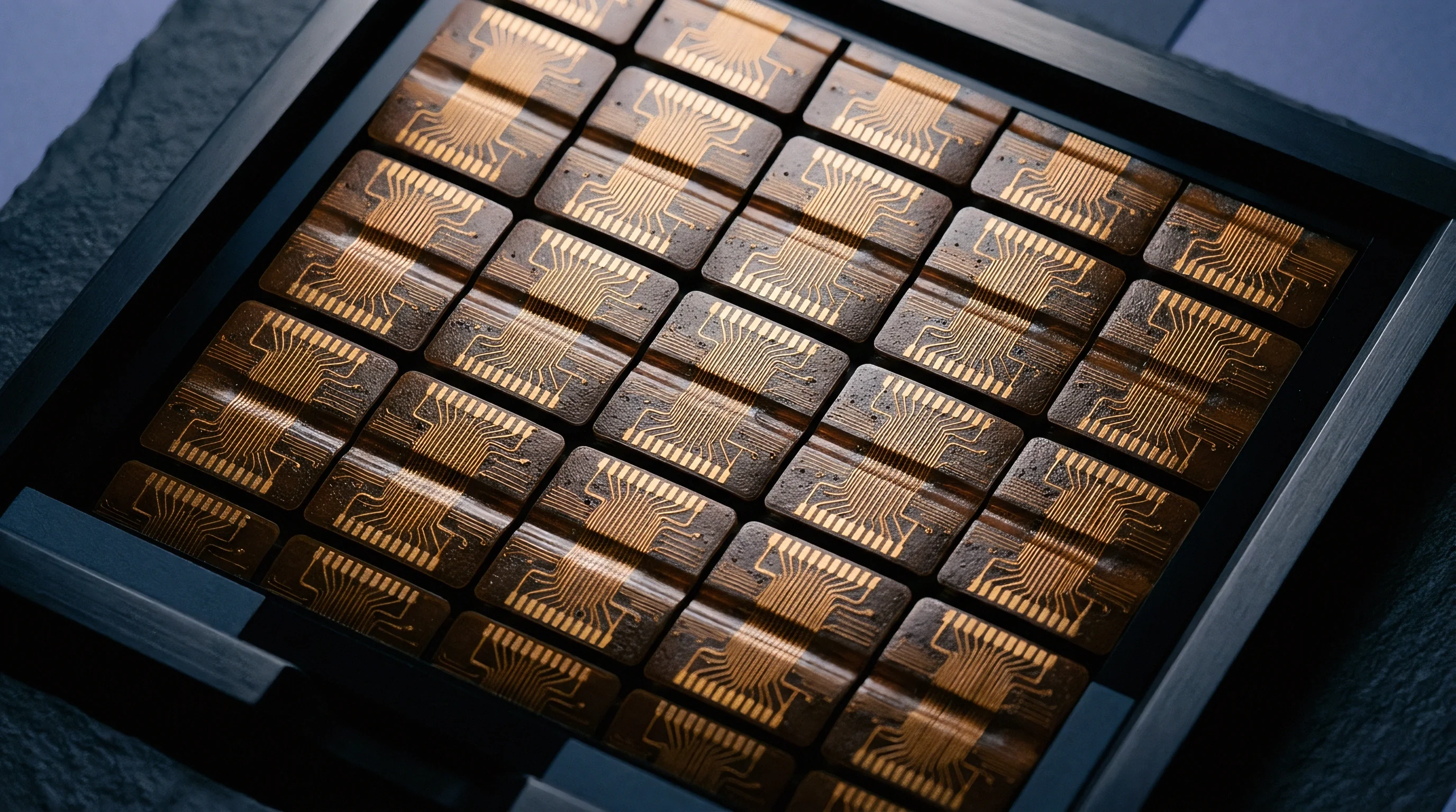
Resin
Substrate core materials dictate RF trace performance through two fundamental properties: relative permittivity and loss tangent. In high-frequency wireless modules operating above 5 GHz, small variations in resin distribution alter transmission line characteristics. High-speed laminates combine woven glass cloth with filled epoxy, hydrocarbon, or PTFE resin systems.
Glass yarn exhibits a relative permittivity near 6.1, while surrounding resin matrices range from 2.1 to 3.2. Local resin-rich or resin-starved zones beneath a microstrip trace create localized impedance discontinuities along the signal path.
Fabrication shops sourcing raw laminate from different material mills introduce subtle material disparities into identical circuit designs. A primary supplier utilizing a spread-glass weave produces uniform dielectric distribution beneath narrow conductors. A secondary fabricator using standard open-weave glass creates periodic dielectric shifts as traces pass over glass bundles and open resin windows.
Glass weave skew alters propagation delay across differential pairs, generating phase imbalance before signal processing components receive the transmission.
Substrate thickness variations compound dielectric constant deviations. A nominal 100-micrometer core thickness varying by 10 micrometers alters characteristic impedance by up to 5 ohms, assuming identical resin content. Fabricators adjust prepreg pressing parameters, temperature ramp rates, and gel times to maintain physical thickness, altering final resin-to-glass ratios.
The resulting laminate meets mechanical dimensions while missing electrical target parameters.
Solder mask application over open RF conductors introduces an uncalibrated dielectric layer that overrides substrate material tolerances.
Dielectric constant shift accelerates signal degradation at higher frequencies. At 28 GHz, a dielectric constant drift from 3.55 to 3.68 shifts the center frequency of a printed bandpass filter by several hundred megahertz. Narrowband matching networks lose efficiency, reflecting power back into the final power amplifier stage.
Thermal dissipation rises while radiated power falls.
Moisture absorption presents another variable between substrate vendors. Hydrocarbon laminates absorb less than 0.06 percent moisture by weight, whereas modified epoxy formulations absorb up to 0.35 percent under humid storage. Water carries a relative permittivity near 70 at room temperature.
Absorbed ambient moisture increases total effective dielectric constant and elevates loss tangent, damping signal amplitudes along long routing paths.
Procuring raw laminates without enforcing strict resin-glass ratios leads to batch rejection during RF end-of-line testing. RF modules fail receiver sensitivity checks when transmission line losses exceed link budget allocations. Scrapped assembled circuit boards represent direct financial loss that primary vendor material certificates fail to cover.


Impedance
Transmission line design relies on predictable conductor geometry and surrounding dielectric properties. Dual sourcing introduces variations in copper foil profile and dielectric thickness that alter effective trace impedance. Electrodeposited copper foils feature higher surface roughness than rolled-annealed foils, extending the physical path length of high-frequency surface currents.
Surface roughness increases effective dielectric attenuation and lowers phase velocity.
Fabricators choose foil types based on internal processing preferences unless engineering drawings specify exact copper profiles. Vendor A applies very low profile electrodeposited copper with a tooth height below 1.5 micrometers. Vendor B selects standard electrodeposited copper with a 3.0-micrometer roughness profile to improve foil-to-resin mechanical adhesion.
This discrepancy shifts trace impedance by 2 to 4 ohms on identical trace widths.
| Parameter | Primary Vendor (ptfe-hydrocarbon) | Secondary Vendor (modified epoxy) | Tolerance Window |
|---|---|---|---|
| Dielectric Constant (10 GHz) | 3.48 | 3.62 | ± 0.05 |
| Dissipation Factor (10 GHz) | 0.0037 | 0.0075 | ± 0.0008 |
| Copper Surface Roughness (Rz) | 1.2 μm | 2.8 μm | Max 1.5 μm |
| Core Thickness Variation | ± 5.0 μm | ± 7.5 μm | ± 5.0 μm |
| Moisture Absorption Rate | 0.04% | 0.20% | Max 0.10% |
Trace width adjustments offset dielectric thickness shifts. When a secondary factory receives artwork designed for a 3.48 dielectric constant, maintaining a 50-ohm line on a 3.62 dielectric substrate demands narrowing line widths. Etching narrower conductors increases DC line resistance and tightens tolerance bounds on chemical processing tanks.
The secondary supplier faces reduced etching yields while trying to hit target RF performance.
Stack-up calculations require explicit modeling of prepreg squeeze flow. Consider a 5.8 GHz microstrip line designed for a 50-ohm target on a nominal 0.200 mm substrate. Material source one provides a substrate with dielectric constant 3.55 and core thickness 0.203 mm, yielding a calculated trace width of 0.442 mm.
Material source two supplies a substrate with dielectric constant 3.68 and thickness 0.191 mm. Achieving 50 ohms on the second material demands a trace width of 0.398 mm, representing an 10 percent width reduction. Applying the first artwork to the second substrate results in a 46.2-ohm line, producing a voltage standing wave ratio of 1.08:1 at the interface.
Stack up Verification Methodology
Cross-section microsectioning reveals structural discrepancies between manufacturing sites. Metallographic preparation confirms actual dielectrics, resin distribution, and copper profile dimensions. Time-domain reflectometry measures impedance profile along the length of test coupons, pinpointing locations where line dimensions vary.
Coupon design must match actual product layer structures exactly to yield valid measurement data.
Tooling adjustments compensate for substrate differences prior to production panel processing. Artwork compensation factors adjust image dimensions on film, offsetting lateral etch bias across different copper weights. Automated optical inspection equipment verifies dry-film resist widths before panel plating and etching operations begin.
Panel layout standardization ensures uniform current density during electroplating processes.
Unresolved impedance mismatch questions remain regarding how thermal expansion cycles alter line capacitance in multi-layer board stacks operating across automotive temperature ranges.


Equivalence
Establishing equivalence between two laminate sources demands verified documentation packages. Design transfers fail when engineering release files contain Gerber geometry alone without raw material specifications. Gerber files describe copper patterns, drill locations, and solder mask boundaries, omitting dielectric constant limits, copper surface finish parameters, and weave styles.
Complete fabrication data requires standardized IPC-2581 or Gerber X2 outputs carrying explicit material properties inside metadata attributes.
Master drawing specifications must establish acceptable alternative materials by specific series name rather than broad IPC slash sheets. An IPC-4101 slash sheet allows wide dielectric constant and loss tangent ranges that span multiple product tiers. Referencing IPC-4101/102 permits materials with dielectric constants ranging from 3.5 to 4.5, a spread far too wide for untuned wireless front-end circuits.
IPC-TM-650 test method 2.5.5.5 split-post resonator verification establishes dielectric constant values at 10 GHz within an absolute uncertainty of plus or minus 0.02.
Fabrication control documentation specifies acceptable core structures, prepreg configurations, and foil profiles. Dual-sourcing strategy requires establishing a baseline qualification protocol for secondary board fabricators.

How Do Fabrication Coupons Validate Second Source Dielectric Performance?
Test coupons embedded in manufacturing panel borders deliver material performance data without destroying production boards. Split-post dielectric resonators measure raw substrate properties prior to processing, while stripline resonator coupons evaluate finished circuit board stacks. Processed coupons capture the combined effect of lamination pressure, thermal cycles, and chemistry exposure on dielectric performance.
Measuring coupon resonant frequencies isolates substrate variations from assembly-induced component placement errors.
- Fabrication Data Files IPC-2581 Level C format files containing explicit stack-up definitions, material properties, and layer assignment attributes.
- Material Specification Sheets Baseline and secondary laminate manufacturer datasheets stating dielectric constant and loss tangent across target operating frequencies.
- Impedance Modeling Reports Field-solver output files establishing trace geometry adjustments for each qualified raw material stack.
- Microsection Analysis Reports Cross-sectional physical measurement records confirming layer thicknesses, copper foil profiles, and glass weave structures.
- Resonator Coupon Data Frequency-sweep test logs measuring effective dielectric constant and insertion loss on finished test panels.
Alternate laminates matching a master drawing slash sheet are often expected to deliver identical RF performance without circuit re-tuning, but slash sheets establish baseline safety limits rather than tight RF performance bands.

Compensation
Circuit layout topology can absorb minor dielectric constant shifts through onboard matching networks. Discrete pi-network topologies positioned between the RF front-end module and the antenna path provide hardware adjustment capabilities. Inductor and capacitor values change across manufacturing runs to realign center frequencies shifted by substrate dielectric drift.
Standard 0201 or 01005 surface-mount passive components offer fine increment tuning steps.
| Substrate Dk Value | Series Inductor (nH) | Shunt Capacitor 1 (pF) | Shunt Capacitor 2 (pF) | Insertion Loss (dB) |
|---|---|---|---|---|
| 3.45 (Low Baseline) | 1.8 | 0.8 | 0.8 | 0.42 |
| 3.55 (Nominal) | 1.5 | 1.0 | 1.0 | 0.38 |
| 3.65 (High Baseline) | 1.2 | 1.2 | 1.2 | 0.45 |
| 3.75 (Out of Spec) | 1.0 | 1.5 | 1.4 | 0.62 |
Software-controlled register trimming compensates for substrate variations in integrated transceiver modules. Internal digital capacitance trim arrays adjust input and output impedance matrices without requiring board modification. Firmware loads trim settings based on batch-level calibration data stored in non-volatile memory during end-of-line production testing.
Trimming expands acceptable raw material dielectric tolerance windows while maintaining product performance requirements.
- Process microsection samples from incoming substrate lot to measure exact dielectric core thickness.
- Perform split-post dielectric resonator testing on un-etched panel edges to verify dielectric constant at target frequency.
- Etch standardized T-resonator coupons included on first production panel to extract effective dielectric constant.
- Calculate matching network component value shifts using verified field-solver models.
- Load batch-specific component placement variants into surface-mount assembly line placement programming.
- Execute full radiated power and receiver sensitivity test suite on initial ten assembled modules.
IPC-6012 Class 3 performance standards mandate maximum dielectric thickness variation limits of plus or minus ten percent across production panels.
Solder mask presence alters RF trace propagation velocity and characteristic impedance. Liquid photo-imageable solder mask exhibits a relative permittivity between 3.3 and 3.8, accompanied by high dissipation factors above 0.02. Mask coverage over transmission lines lowers overall impedance by 1 to 3 ohms compared to bare copper lines.
Modern RF layouts utilize solder mask keep-out windows over high-frequency paths to eliminate mask tolerance variables entirely.
Specifying IPC-6012E Class 3 production rules locks fabricators into tight dielectric layer thickness tolerances, shifting standard manufacturing acceptance limits from ten percent down to five percent.

Settlement
Commercial contracts define financial responsibility for scrap generated by dielectric material drift. Primary suppliers guarantee panel delivery against mechanical drawings and basic IPC slash sheets. Standard board supply contracts contain no explicit RF performance guarantees unless custom acceptance criteria enter the master purchase agreement.
RF yield losses remain the buyer’s liability when bare boards meet IPC visual and continuity requirements.
- Unspecified Material Substitutions Fabricator switches prepreg weave or resin system without written engineering change authorization, causing RF detuning.
- Etching Tolerance Accumulation Conductor width variations combined with high dielectric constant cores push trace impedance outside specification bounds.
- Copper Profile Oversights Uncontrolled foil roughness increases attenuation beyond link budget allowances, triggering module rejection.
- Inadequate Coupon Verification Panel borders lack standardized RF test structures, preventing non-destructive material quality verification.
Establishing engineering change order thresholds prevents unannounced material shifts. Contracts must define a mandatory process change notification trigger for any shift in resin formulation, glass style, copper foil supplier, or nominal core thickness. Fabrication vendors failing to issue notifications bear full financial responsibility for assembled board scrap, re-engineering hours, and test line downtime.
Dual-sourcing RF substrates successfully relies on translating electrical tolerances into tight fabrication drawings, enforcing panel-level coupon testing, and structuring commercial terms around verified RF yields rather than bare-board continuity checks.