Managing Orthogonal Thermal Strain Mismatch in Multi-Material Precision Structures
Managing orthogonal thermal strain mismatch requires matching material expansion axes and using kinematic flexures to decouple multi-axis stress.
Vector
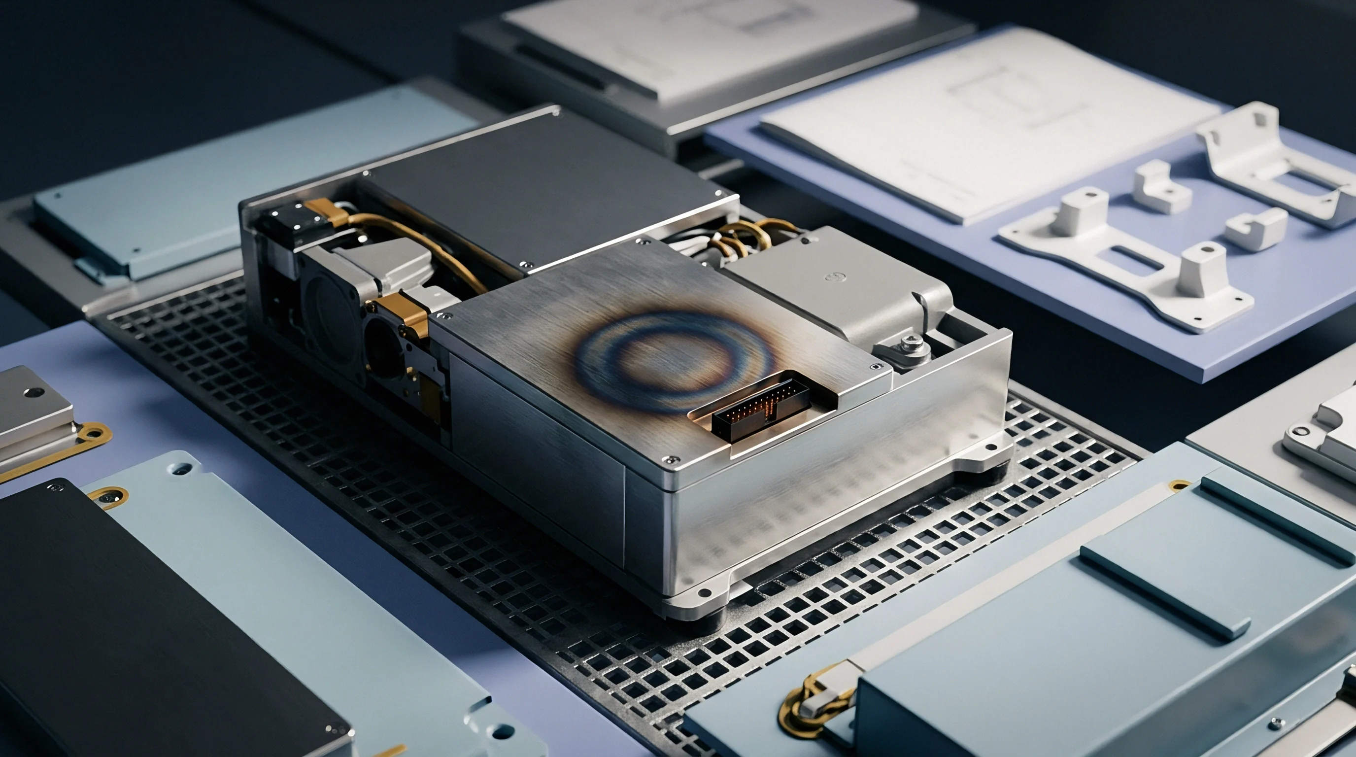
Planar thermal expansion coefficients rarely match normal expansion rates in stratified radio-frequency modules. A high-frequency laminate exhibits twelve to sixteen parts per million per kelvin along its horizontal copper plane, while its out-of-plane axis expands at forty-five to seventy parts per million per kelvin. When a gallium nitride bare die sits atop a copper-molybdenum-copper flange via gold-tin eutectic solder, this three-dimensional divergence dictates mechanical survival.
Thermal dissipation forces heat down through the stack, producing steep temperature gradients across sub-millimeter distances. Differential movement between axes creates severe twisting moments across peripheral solder interconnects.
Reference designs distributed by semiconductor foundries routinely assume infinite, unconstrained copper heat spreaders beneath evaluation boards. Those layouts work fine during brief bench tests in open ambient air, but real systems enclose modules inside sealed aluminium or kovar enclosures where heat sinks face boundary airflow resistance. The resulting equilibrium temperature causes the laminate to swell vertically three times faster than it stretches laterally.
Microstrip traces lift away from internal ground planes, changing characteristic impedance by up to eight ohms at twenty-eight gigahertz as warping breaks peripheral ground continuity.
Under steady seventy-watt dissipation, an unrestrained brass carrier produces twelve micrometers of edge deflection across a forty-millimeter span.
Engineers purchasing turnkey assemblies encounter catastrophic field detachments when suppliers overlook anisotropic coefficient profiles. Low-cost substrate suppliers frequently quote only the in-plane expansion figure on catalog sheets. Glass-weave reinforcement constrains movement across the woven fabric directions while resin swells unrestricted along the perpendicular thickness.
Dielectric constants change dynamically under cyclic strain, shifting the tuned phase characteristics of quadrature hybrid couplers ~ where a phase shift of four degrees destroys carrier cancellation in Doherty power amplifier topologies.
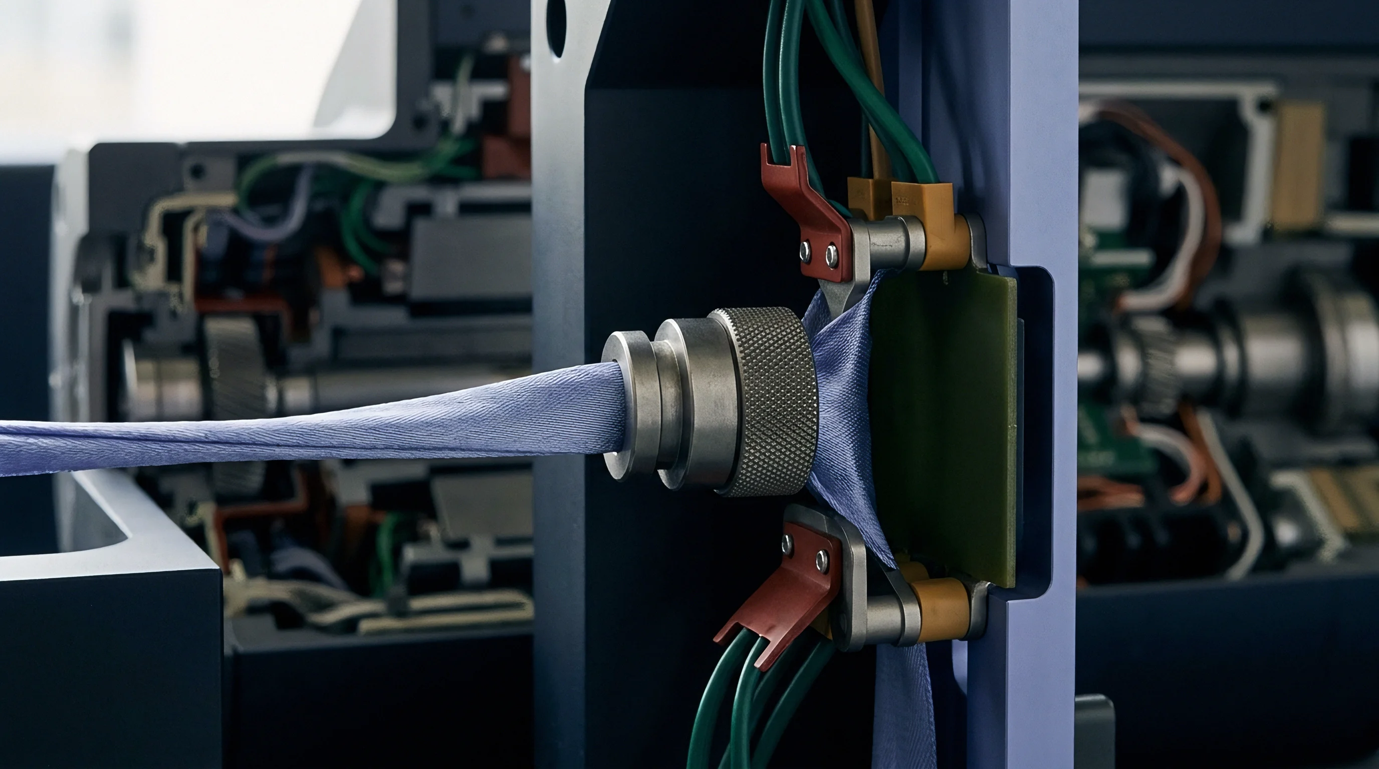
Mechanical stress profiles partition into normal and shear components across bonded interfaces. When lateral expansion generates high shear strain at the corners of a wide component, vertical expansion introduces tensile peel stresses along the solder perimeter, accelerating crack propagation along intermetallic compound boundaries. Because gold-tin solder creeps very slowly, solder fatigue drives interface cracking.
Neglecting this multi-axis interaction during structural finite element analysis results in rapid delamination of RF die attachments and total signal transmission loss.
Joint
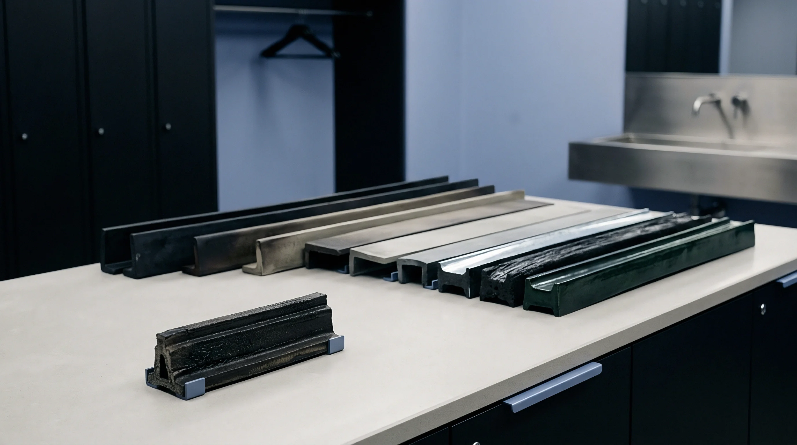
Bond lines operate as the sole mechanical accommodation layer between components with irreconcilable thermal properties. Sintered silver paste provides eighty watts per meter-kelvin of thermal conductivity with an elastic modulus exceeding fifty gigapascals, forming porous networks. When placed between an aluminium nitride submount and a thick copper pedestal, the sintered joint experiences severe cyclic shear.
Gold-tin eutectic joints operate at higher temperatures but remain brittle, transferring strain directly into delicate semiconductor layers rather than yielding plastically.
Will Anisotropic Solder Stiffening Provoke Interfacial Fracture?
Intermetallic growth between tin-based alloys and substrate metallizations consumes compliant bulk material during thermal aging. Over two thousand thermal cycles between minus forty and plus one hundred twenty-five degrees Celsius, nickel-tin intermetallic layers grow to four micrometers in thickness. These compounds possess fracture toughness values below two megapascals per square root meter.
Every interface stores elastic energy, and normal expansion along the substrate thickness continuously pulls on these brittle reaction layers, converting lateral shear displacement into catastrophic peeling fractures.
| Material Designation | In-Plane Expansion | Thickness Expansion | Tensile Modulus | Thermal Conduction |
|---|---|---|---|---|
| Gallium Nitride on Silicon Carbide | 3.8 ppm/K | 3.8 ppm/K | 420 GPa | 380 W/m-K |
| Copper-Molybdenum (85/15) | 7.2 ppm/K | 7.2 ppm/K | 280 GPa | 190 W/m-K |
| Woven PTFE RF Laminate | 12.0 ppm/K | 52.0 ppm/K | 1.2 GPa | 0.6 W/m-K |
| Eutectic Gold-Tin (80/20) | 16.0 ppm/K | 16.0 ppm/K | 59 GPa | 57 W/m-K |
| Aluminium Nitride Ceramic | 4.5 ppm/K | 4.5 ppm/K | 310 GPa | 170 W/m-K |
Adhesive interposers introduce compliance at the direct penalty of thermal impedance. Filled silicone adhesives yield readily, protecting ceramic optical benches from distorted structural housings, but their thermal conductivity remains below two watts per meter-kelvin. Micro-radian alignment tolerances in laser diode packages collapse when soft adhesives creep under continuous preloads while thermal pads relax under compression.
When procurement teams negotiate module builds, selecting the attachment medium dictates long-term positional stability across thousands of power cycles.
- Intermetallic compound embrittlement occurs along the interface between copper pads and high-tin alloys, eliminating strain compliance and accelerating brittle crack initiation under combined shear and out-of-plane tensile loads.
- Dielectric layer fracture develops within low-k semiconductor stacks when stiff eutectic joints transmit thermal envelope movements directly into brittle silicon dioxide and gallium arsenide films.
- Solder void agglomeration concentrates multi-axis stresses around localized thermal hotspots, tripping thermal protection circuits and detuning high-frequency transistor matching networks.
- Bond wire heel necking proceeds from persistent differential lift-off as substrates expand vertically faster than surrounding metal lead frames during transient temperature spikes.
Contract manufacturing facilities often dismiss early microcracks as cosmetic fillet irregularities during initial acoustic microscopy reviews, only for production yields to fall below target. Post-reflow solder joint cracking is frequently attributed to customer over-temperature exposure rather than improper substrate metallurgy selection.


Tolerance
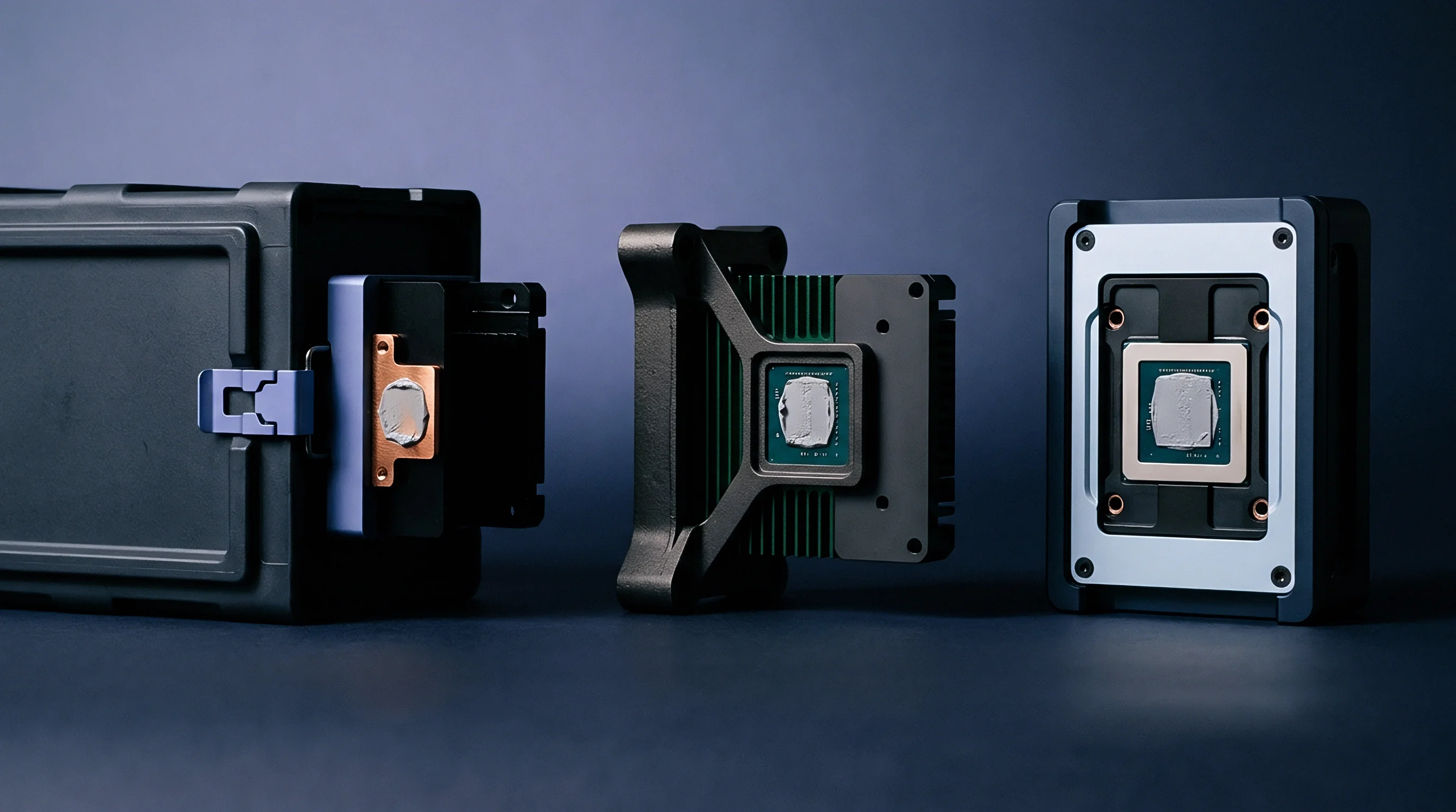
Geometric dimensioning standards isolate kinematic movement paths across precision structural frames. A traditional bolted connection forces two components to share displacement coordinates across planar surfaces, generating high frictional locking forces. Kinematic mounts rely on exact constraint principles, establishing contact through six deterministic points across grooves or spherical cups.
Differential expansion between a titanium carrier and a fused silica prism produces pure radial motion along guide vectors without inducing bending moments that lead to axial drift and broken optical coupling.

Alignment Stability across Environmental Temperature Swings
Deflection budgets in electro-optical packages dictate micro-radian angular tolerances across operating bands. When an optical fiber array couples to a photonic integrated circuit, lateral displacements exceeding five hundred nanometers attenuate optical signal power by three decibels. In-plane expansion shifts the relative centerlines of optical waveguides, while vertical expansion tilts the collimating lenses.
Monolithic flexures cut via wire electrical discharge machining decouple the expansion of external housing walls from the isolated optical carrier plate.
Per IPC-SM-785 section 5.4, thermal fatigue life claims require power cycling validation under representative thermal gradient conditions.
Thermal isolation requires careful balance against structural resonance frequencies. Thin flexure blades provide low thermal-mechanical stiffness along the expansion vector, yet they lower mechanical resonant frequencies. A structure exposed to vehicular vibration requires high stiffness to prevent harmonic displacement during transit.
Tooling wear alters machining tolerances on flexure blade thickness, directly changing stiffness by the third power of beam thickness.
| Flexure Configuration | Material Base | Thermal Radial Drift | Angular Tilt | First Resonance |
|---|---|---|---|---|
| Monolithic Three-Blade Leaf | Titanium Grade 5 | 0.35 um | 1.2 urad | 1450 Hz |
| Cantilever Kelvin Joint | Invar 36 | 0.12 um | 0.8 urad | 1120 Hz |
| Slotted Planar Diaphragm | Beryllium Copper | 0.82 um | 4.1 urad | 890 Hz |
| Dual-Axis Parallel Flexure | Stainless Steel 316L | 1.15 um | 5.6 urad | 760 Hz |
Procuring custom flexure structures requires exhaustive coordinate measuring machine dossiers. A variation of five micrometers in flexure centerlines shifts the thermal neutral axis of an optical assembly, causing asymmetrical angular deviation during heating when rigid adhesives transfer stress directly. Sourcing specifications mandate that suppliers verify flexure spring rates and neutral axis positions on production qualification lots before shipment release.
Failure to specify non-destructive acoustic evaluation clauses in master service agreements transfers all financial liability for substrate delamination directly onto the purchasing organization.


Transfer
Manufacturing packages for multi-material structures demand documentation far beyond standard Gerber data and bills of materials. Detailed packages convey the complete layer-by-layer copper area distributions to balance thermal warpage across reflow profiles, as copper balance dictates final bow. Symmetrical dielectric stackups prevent board curling during wave soldering and surface mount assembly.
Missing layer-by-layer copper area coverage details in the fabrication documentation guarantees uneven warpage and subsequent solder bridge defects across fine-pitch land grid arrays.
Whose Acceptance Test Governs Substrate Delamination?
Assembly yield debates arise when receiving departments inspect incoming multi-layer modules using differing environmental test fixtures. A component vendor tests flat bare packages on heated plates, observing uniform expansion across planar geometries. The buyer installs modules into cast chassis with perimeter fasteners, triggering three-dimensional saddle distortions during thermal ramp tests where die shear tests reveal microcracks.
Unless contract documentation specifies exactly how modules must be mechanically constrained during post-assembly acceptance testing, neither party can enforce warranty claims.
A symmetric copper distribution across dielectric layers prevents reflow warpage from exceeding the IPC-A-610 Class 3 limit of point seven five percent.
Dual-sourcing precision assemblies requires re-qualifying raw material batch properties when secondary suppliers recalculate thermal expansion. A second factory may employ laminate prepregs with slightly different resin contents, shifting out-of-plane expansion coefficients by fifteen percent. As thermal cycles induce plastic deformation, even identical electrical schematics cannot prevent mechanical changes in prepreg types from rupturing peripheral solder balls on large area array packaging.
- The design house delivers full step-and-repeat mechanical drawings, three-dimensional finite element model geometry files, and exact metallization stackup thicknesses to the lead assembly facility.
- Tooling engineers construct custom assembly carriers with thermal expansion coefficients calibrated to clamp modules securely without introducing compressive mechanical preloads during solder reflow.
- Process technicians evaluate initial reflow runs using shadow moire interferometry across the temperature profile from twenty-five to two hundred sixty degrees Celsius, mapping full-field warpage behavior.
- Quality personnel verify that out-of-plane package warpage remains strictly beneath seventy-five micrometers across all coordinate directions, preventing solder bridging and open joint formations.
Unresolved questions persist regarding whether dynamic acoustic imaging during active RF power cycling can distinguish between benign substrate delamination and catastrophic active die detachments before thermal runaway destroys the underlying gate metallization.

Margin
Commercial contracts define who absorbs financial losses when thermal strain mismatches lower assembly yields. Turnkey manufacturing quotes present attractive fixed-price structures, but design changes prompted by field delamination trigger massive non-recurring engineering renegotiations. Building custom kinematic packaging involves extensive five-axis machining and tight material certification processes, where joint stiffness shifts dynamic resonance.
A semi-custom integration boundary allows the buyer to retain design ownership of critical structural interfaces while subcontracting high-volume component assembly.
Balancing Engineering Scope against Manufacturing Investment
Specifying custom materials alters supply lead times and minimum purchase volumes. Machining Invar 36 carriers requires specialized tooling and slow cutting speeds, increasing non-recurring engineering expenses by thirty-five percent over standard aluminium carriers. Material lead times expand from six weeks to twenty-two weeks when procuring controlled-expansion alloys, forcing sourcing teams to analyze whether module performance justifies the prolonged inventory carrying costs and stringent quality audits.
| Integration Model | Tooling Ownership | NRE Investment | Change Control | Exit Penalty |
|---|---|---|---|---|
| Turnkey Standard | Factory Retained | Low ($5k-$15k) | Vendor Controlled | High Tooling Loss |
| Semi-Custom Carrier | Shared Allocation | Medium ($25k-$60k) | Joint Sign-Off | Moderate Re-Tooling |
| Build-to-Print Kinematic | Buyer Owned | High ($80k-$200k) | Buyer Controlled | Low Transfer Friction |
Purchasing agreements require clear clauses governing raw material batch certifications. When an unannounced mill change alters the carbon content in an Invar shipment, its thermal expansion coefficient shifts from one point two to three point eight parts per million per kelvin. That variation doubles thermal drift in precision resonator cavities, pushing operating frequencies outside regulated spectrum bands.
- Mechanical drawing custody establishes buyer ownership over all native computer-aided design files, step models, and geometric tolerance schemes, preventing vendor lock-in when secondary manufacturing sites are needed.
- Material traceability dockets require certified mill test reports detailing expansion coefficients and chemical compositions for every metal billet, ceramic plate, and prepreg roll used in production.
- Part change notification windows enforce a mandatory ninety-day technical review period before a contract manufacturer can substitute adhesives, solder alloys, or substrate vendors.
- Reflow warpage guarantees tie payment milestones directly to shadow moire surface topography compliance across the entire operating thermal profile.
Thermal stability requires mechanical compliance to sit at the lowest stiffness interface in the assembly stack.