Oscillator Drift Parameters in Low Duty Cycle Radios
Oscillator drift forces wider receiver listen windows in low duty cycle radios, multiplying active energy consumption and degrading battery lifespan.
Quartz
Low duty cycle wireless nodes spend over ninety-nine percent of their operational lifespan in sleep modes to conserve primary cell battery energy. During these quiescent intervals, the high-frequency Phase-Locked Loop and main system clock shutdown completely, leaving a low-power secondary oscillator to keep track of network time. This dual-clock architecture establishes a fundamental dependency between physical crystal properties and system energy consumption.
Oscillator Physics in Duty Cycle Architecture
Power dissipation in battery-operated telemetry hardware forces microcontrollers into deep sleep states. In these states, current draw drops from milliamperes down to sub-microampere levels. The primary high-frequency oscillator, typically utilizing an AT-cut quartz crystal operating between 16 MHz and 32 MHz, consumes several hundred microamperes merely sustaining mechanical resonance.
Consequently, the system disables the high-frequency crystal driver during sleep and delegates baseline timing to a low-frequency oscillator running at 32.768 kHz.
Low-frequency 32.768 kHz crystals typically employ a tuning-fork mechanical geometry. This structure achieves high physical resonance stability at minimal drive power, often below one microwatt. Sleep current dictates battery life.
However, tuning-fork quartz cuts exhibit a parabolic frequency-temperature characteristic centered around twenty-five degrees Celsius. The fractional frequency variation follows a quadratic equation where temperature deviations above or below the turnover point reduce the resonant frequency.
The parabolic frequency shift is expressed by the coefficient k, typically measured at minus 0.035 parts per million per degree Celsius squared. At an operating temperature of minus twenty degrees Celsius, the temperature differential of forty-five degrees from the turnover point produces a frequency shift of minus seventy-one parts per million. At positive sixty degrees Celsius, the shift reaches minus forty-three parts per million.
This physical limitation means an uncompensated tuning-fork oscillator runs slower at both low and high temperature extremes.
Sleep Clock versus High Frequency Synthesizer
Timing architecture in low power radios relies on two distinct frequency sources operating at different operational phases. The 32.768 kHz sleep clock governs sleep interval duration, wake-up scheduling, and initial preamble window timing. When the node wakes to transmit or receive, the high-frequency AT-cut crystal synthesizes the Radio Frequency carrier and baseband clocking.
High-frequency AT-cut crystals display a third-order cubic frequency-temperature curve rather than a parabolic curve. Their frequency deviation stays within plus or minus ten to thirty parts per million across the industrial temperature band of minus forty to positive eighty-five degrees Celsius. High-frequency oscillator drift shifts the actual channel frequency away from nominal channel center, introducing Carrier Frequency Offset at the receiver RF front end.
Thermal parabolic curvature in low-frequency sleep oscillators dominates sleep timing error at environmental temperature extremes.
Tuning fork crystals also carry an initial calibration tolerance at room temperature, typically specified between plus or minus ten and plus or minus thirty parts per million. Parasitic board capacitance skews sleep timing. External load capacitors, trace layout capacitance, and microcontroller pin input capacitance shift the actual oscillation frequency away from nominal resonance.
Silicon vendors frequently attribute missing packet sync during cold-weather field operation to uncalibrated PCB trace capacitance rather than component tolerances.

Tolerance
Frequency deviations accumulate continuously while the radio baseband processor slumbers between scheduled network communication slots. In synchronized duty-cycle protocols, both the transmitter and receiver experience independent oscillator drift during the sleep interval. The total time uncertainty between two nodes scales linearly with sleep duration and total effective frequency tolerance.
Cumulative Timing Slip over Sleep Intervals
Extended sleep durations exacerbate timing offset between end nodes and gateway receivers. Total frequency error represents the linear sum of four distinct components: initial room-temperature tolerance, temperature-induced drift, aging drift over time, and supply voltage pushing effects. A standard low-cost tuning fork crystal presents a baseline tolerance of plus or minus twenty parts per million at production assembly.
When operating across a wide thermal range, thermal curvature adds up to seventy-five parts per million of offset. Crystal aging contributes an additional three to five parts per million in the first operating year. Power supply fluctuations across battery discharge cycles add another two parts per million.
Under worst-case combined conditions, total low-frequency sleep clock uncertainty reaches one hundred parts per million.
For a radio sleeping for ten seconds between poll intervals, a one hundred parts per million total timing error produces one millisecond of time shift. If the node slumbers for one hour, the cumulative timing slip reaches three hundred sixty milliseconds. The receiving node must open its active listening window early enough to absorb this full temporal offset, spending high active current while waiting for the transmitter preamble to arrive.

Frequency Deviation Mechanics across Sub-GHz and 2.4 GHz
Carrier frequency shifts affect narrow-band channels more severely than wide-band spread spectrum modulations. A thirty parts per million frequency offset on a 2.4 GHz carrier creates a seventy-two kilohertz physical frequency displacement. In a standard Bluetooth Low Energy system with one megahertz channel spacing, seventy-two kilohertz remains comfortably within the channel filter bandwidth.
In sub-GHz industrial networks operating on 154 kHz or 25 kHz narrow-band channels, carrier frequency offset shifts the signal onto the steep skirt of the receiver channel filter. An 868 MHz sub-GHz link experiencing thirty parts per million carrier drift incurs a twenty-six kilohertz shift. On a 12.5 kHz channel, this offset moves the incoming RF signal completely outside the receiver passband, destroying link connectivity regardless of transmit output power.
Uncompensated oscillator drift creates predictable failure mechanisms across low duty cycle radio deployments:
- Synchronization loss during receive wake causes the node to miss the base station beacon entirely, triggering full rejoin cycles.
- Carrier frequency offset beyond filter band attenuates incoming RF energy by pushing the signal onto the channel filter slope.
- Preamble truncation under timing slip reduces available symbol integration time, elevating bit error rate under weak field coverage.
- Overlapping transmission collision occurs when node wake timing drifts into adjacent time-division channel slots assigned to neighbor devices.
The selection of oscillator hardware directly dictates total timing accuracy and sleep current budgets across operational environments.
| Oscillator Type | Nominal Frequency | Initial Frequency Spread | Thermal Spread (-40C to +85C) | Typical Sleep Power | Primary Use Case |
|---|---|---|---|---|---|
| Standard Tuning Fork Crystal | 32.768 kHz | +/- 20 ppm | -80 to 0 ppm | 0.5 uW | Basic low-cost sensor nodes |
| Temperature-Compensated Sleep Clock | 32.768 kHz | +/- 5 ppm | +/- 5 ppm | 1.5 uW | Long-interval synchronized nodes |
| Standard AT-Cut Quartz Crystal | 32.000 MHz | +/- 10 ppm | +/- 25 ppm | 600 uW (Active) | Standard RF carrier synthesis |
| High-Precision RF TCXO | 32.000 MHz | +/- 0.5 ppm | +/- 2 ppm | 2.5 mW (Active) | Ultra-narrowband sub-GHz radios |
Selecting uncompensated sleep components for long-interval telemetry devices forces battery replacement schedules forward by years due to expanded receiver power cycles.

Window
Receiver open duration directly dictates average system current in low power radio nodes operating scheduled downlink polling. When nodes rely on periodic reception windows, the receiver must activate before the expected packet arrival time to guarantee capturing the preamble sequence. Clock uncertainty forces the receiver to open this window prematurely, spending energy on quiet air.
How Do Frequency Tolerances Expand RX Windows?
Guard bands expand scheduled reception slots to prevent packet synchronization failures caused by clock drift. Receiver arrival time uncertainty is symmetric, requiring early activation and extended timeout windows. The minimum mandatory receiver guard time calculation combines total sleep duration, transmitter clock tolerance, and receiver sleep clock tolerance.
Uncertainty forces wider listen windows. If transmitter clock drift equals twenty parts per million and receiver clock drift equals fifty parts per million, the maximum relative frequency difference reaches seventy parts per million. Multiplying seventy parts per million by the sleep duration defines the single-sided timing uncertainty.
The radio must double this value to account for drift in either positive or negative time directions.
Baseband clocks slip during sleep. In addition to raw crystal drift, digital baseband timer quantization introduces fixed timing steps. If the sleep clock operates from an internal RC oscillator running at 32 kHz, single-period quantization adds thirty-one microseconds of clock uncertainty on every wake event.

Mathematical Guard Band Formulation and Worked Energy Penalty
Calculating total timing guard requires accounting for transmitter drift, receiver drift, and baseband phase lock delay. Consider an industrial sensor node operating on a LoRaWAN Class A downlink pattern or a Time-Synchronized Channel Hopping network. The transmitter exhibits a timing drift parameter denoted as delta-T-tx, while the receiver exhibits delta-T-rx.
The mathematical total receive window duration T-rx-window is expressed as:
T-rx-window = T-preamble + 2 (T-sleep (PPM-tx + PPM-rx) 10^-6) + T-lock
Where T-preamble represents the physical time required to detect and lock onto the radio preamble, T-sleep represents total sleep duration in seconds, PPM-tx and PPM-rx represent respective clock tolerances, and T-lock represents internal synthesizer stabilization delay.
To quantify the financial and battery impact, analyze a concrete scenario featuring a sub-GHz telemetry radio node. Assume the node wakes every 128 seconds to poll for downlink configuration commands. The radio receiver draws 12.0 milliamperes in active receive mode from a 3.6 Volt primary Lithium Thionyl Chloride battery.
The physical preamble detection length requires 4.0 milliseconds of clean signal.
Under ideal conditions with zero clock drift, the receiver opens for exactly 4.0 milliseconds per cycle. The daily energy spent on downlink reception equals 675 wake cycles multiplied by 4.0 milliseconds multiplied by 12.0 milliamperes at 3.6 Volts, yielding 2.33 Joules per day.
Now evaluate the real-world condition where the transmitter uses a 20 ppm clock and the receiver uses an uncompensated 32.768 kHz tuning fork crystal subject to outdoor thermal swings. At minus ten degrees Celsius, the combined clock error reaches 80 ppm. Calculating the timing guard band over the 128-second sleep interval yields:
Guard-Band = 2 (128 80 10^-6) = 20.48 milliseconds
Adding the 4.0 millisecond preamble lock requirement results in a total active receive window duration of 24.48 milliseconds per cycle. Active current consumption during each window remains 12.0 milliamperes. Daily energy consumption for downlink listening increases to:
Daily-Energy = 675 0.02448 seconds 0.012 Amperes 3.6 Volts = 7.14 Joules per day
A clock drift of one hundred parts per million during a ten-minute sleep interval expands the mandatory receiver guard band by one hundred twenty milliseconds.
Frequency offsets destroy link margin. Over a ten-year target operating lifecycle, energy consumed solely by downlink reception rises from 8,504 Joules under zero drift up to 26,061 Joules under 80 ppm drift. The 17,557 Joule energy penalty equates to 1,354 milliampere-hours of extra battery capacity.
On a standard 1/2 AA cell rated at 1,200 milliampere-hours, clock drift completely exhausts the battery years before its expiration date.
| Radio Standard | Sleep Interval | Total Clock Drift | Receiver Active Current | Mandatory RX Guard Band | Annual Battery Energy Drag |
|---|---|---|---|---|---|
| LoRaWAN SF12 (125 kHz) | 128 s | 30 ppm | 11.5 mA | 7.68 ms | 11.4 kJ |
| LoRaWAN SF12 (125 kHz) | 128 s | 100 ppm | 11.5 mA | 25.60 ms | 38.1 kJ |
| BLE Coded PHY (S=8) | 1.28 s | 50 ppm | 8.2 mA | 0.128 ms | 7.2 kJ |
| TSCH 802.15.4e (Slot 10ms) | 10.0 s | 20 ppm | 5.5 mA | 0.400 ms | 0.8 kJ |
| NB-IoT eDRX Cycle | 20.48 s | 15 ppm | 40.0 mA | 0.614 ms | 10.3 kJ |
Phase noise degrades receiver sensitivity. Narrow filters require accurate clocks. Cold temperatures drop output frequency.
Tight tolerances extend active runtime. Preamble detection fails under offset. Designing receive window guard bands around room temperature oscillator tolerances guarantees premature field failure in outdoor deployments.
Expense
Silicon selection and bill of materials trade-offs dictate the economic viability of ultra-low-power radio module designs. Engineering teams frequently compare component unit prices on the immediate hardware purchase order without factoring in the lifetime enclosure and primary cell battery sizing costs.

Component Price Differences versus Lifetime Battery Sizing
Selecting high-precision timing components adds upfront hardware cost while reducing battery capacity needs. A standard 32.768 kHz tuning fork crystal with plus or minus twenty parts per million tolerance costs approximately six cents in production quantities. Upgrading to an integrated Temperature-Compensated Crystal Oscillator increases unit component cost to sixty cents.
This fifty-four cent hardware premium alters system-level economics favorably when evaluated against energy density costs. As demonstrated in receive guard band calculations, high clock drift forces the addition of an extra 1,350 milliampere-hours of primary battery capacity to achieve a ten-year operational lifetime. A primary A-size Lithium Thionyl Chloride battery rated at 3,600 mAh costs approximately two dollars and forty cents, whereas a C-size cell rated at 8,500 mAh costs over five dollars.
Spending fifty-four cents on a temperature-compensated sleep oscillator eliminates two dollars and sixty cents in battery chemistry costs. Furthermore, smaller battery footprint requirements reduce protective enclosure dimensions, lowering injection molding tool costs and freight fees.
Procurement Specification Directives for Oscillator Selection
Engineering requirements written into sourcing documentation prevent performance degradation from unvetted component changes. Module qualification protocols specify rigid limits on frequency tolerance, temperature drift, and aging parameters.
Purchasing specifications must include mandatory verification criteria before approving alternate crystal suppliers:
- Crystal load capacitance match verification confirms that stray PCB pad capacitance matches vendor specifications within half a picofard.
- Parabolic temperature coefficient specification defines maximum acceptable frequency curvature over specified outdoor operating temperature limits.
- Maximum allowable aging rate declaration limits long-term frequency drift to under three parts per million during the first operational year.
- High-frequency crystal drive level cap prevents mechanical stress damage and premature resonance degradation inside compact radio packages.
Evaluating trade-offs across oscillator topologies helps balance initial bill-of-materials costs against total device lifecycle costs.
| Component Architecture | Oscillator BOM Cost | Sleep Drift Budget | Required Battery Capacity | Battery Cell Cost | Net System Hardware Cost |
|---|---|---|---|---|---|
| Uncalibrated Tuning Fork Crystal | $0.06 | 110 ppm | 3,600 mAh | $2.40 | $2.46 |
| Calibrated Quartz + Software Temp Compensation | $0.12 | 35 ppm | 1,800 mAh | $1.50 | $1.62 |
| Integrated Sleep TCXO (32.768 kHz) | $0.60 | 5 ppm | 1,200 mAh | $1.10 | $1.70 |
| High-Precision HF TCXO + Sleep Calibrated | $1.10 | 2 ppm | 1,000 mAh | $0.95 | $2.05 |
Investing in tighter sleep clock tolerances reduces battery cell physical volume more effectively than adding raw chemical storage capacity.
Contractual supply agreements specifying maximum oscillator frequency deviation across temperature protect module buyers from unannounced crystal vendor substitutions.
Audit
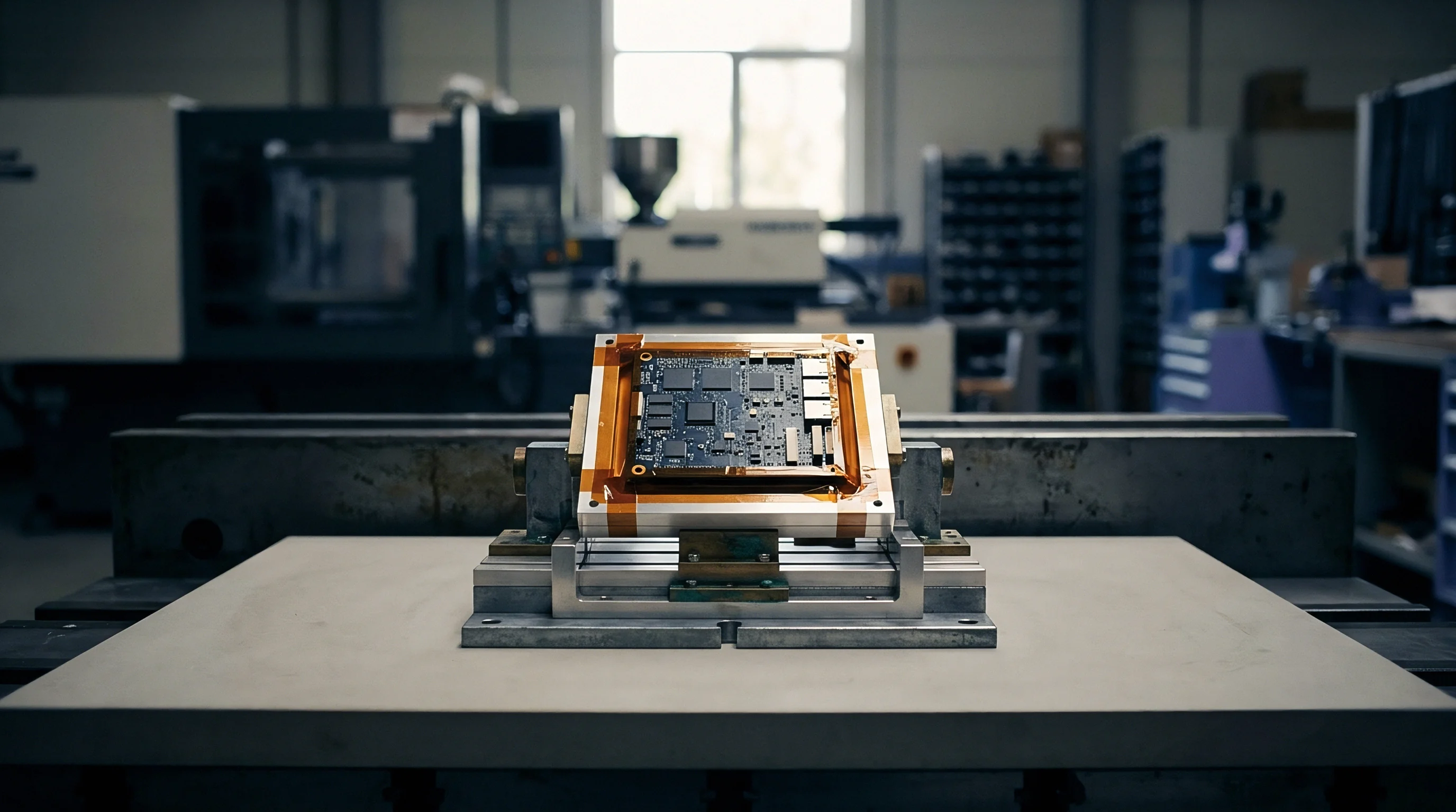
Bench measurement of low-frequency sleep clocks demands high-impedance buffered test setups to prevent probe loading distortion. Standard passive oscilloscope probes add ten picofarads of capacitance in parallel with the oscillator circuit. Attaching a standard probe to a 32.768 kHz quartz node alters the resonant frequency by tens of parts per million or stops oscillation entirely.
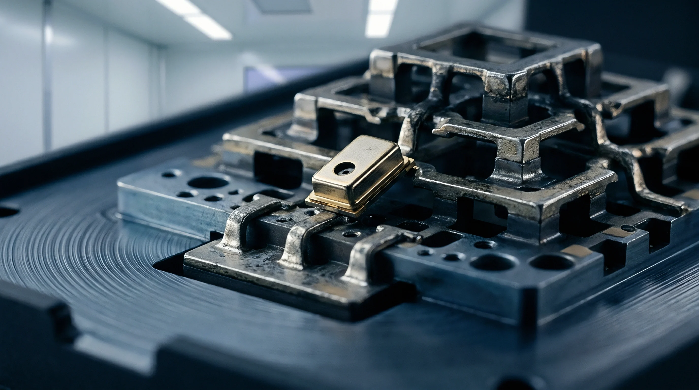
Bench Testing Sleep Oscillators without Circuit Loading
Direct physical attachment of oscilloscope probes introduces parasitic capacitance that alters resonant frequency. Engineers evaluate sleep clock performance by routing internal clock signals to dedicated microcontroller GPIO output buffers. Configuring internal clock output registers isolates the sensitive oscillator core from external test equipment loading.
Alternatively, non-contact near-field magnetic probes capture oscillator emissions without physical contact. The high-impedance signal feeds into a high-precision frequency counter locked to a rubidium or GPS-disciplined atomic frequency standard. Measuring frequency deviation across thermal chambers reveals true component parabolic performance curves.
Production Thermal Profiling and Firmware Offset Calibration
Factory test lines eliminate fixed manufacturing frequency offsets through non-volatile memory register calibration. During automated board testing, the tester measures sleep clock frequency at room temperature and calculates the initial calibration error. Microcontrollers write this offset value into internal Flash memory, enabling real-time software counter adjustments.
The following sequence establishes production testing protocols for low duty cycle radio clock verification:
- Route the internal low-frequency sleep clock to a buffered output test pin using microcontroller register configuration without attaching direct passive probes.
- Connect the buffered output pin to a high-precision frequency counter locked to a rubidium or GPS-disciplined reference clock source.
- Place the device under test inside an environmental chamber and stabilize temperature at twenty-five degrees Celsius for fifteen minutes.
- Measure initial frequency offset, calculate offset calibration register value, and flash calibration constants into non-volatile device storage.
- Sweep chamber temperature from negative forty to positive eighty-five degrees Celsius to verify parabolic temperature compensation firmware curves.
Compliance with European Telecommunications Standards Institute EN 300 220 requires transmitter center frequency error to remain within specified channel boundaries under extreme supply voltage.
Guard time consumes active energy. Thermal shifts expand arrival times. Load capacitance alters oscillator frequency.
Parasitic capacitance skews sleep timing. Whether automated single-point factory calibration provides sufficient long-term drift mitigation as crystal aging effects compound over decade-long deployments remains an open question for module buyers.