Silicon Substrate Trap Layers for RF Linearity Control
Polysilicon trap layers suppress substrate carrier inversion to maintain high RF linearity, eliminating harmonic leakage across multi-band front-end switches.


Charge
Direct current test probes touching a bare high-resistivity silicon wafer register bulk resistivities exceeding 3,000 Ohm-centimeters, yet radio frequency signals passing through an integrated switch core built above that same silicon encounter an effective resistivity below 30 Ohm-centimeters. This discrepancy stems from fixed positive charges within the overlying thermal silicon dioxide layer, typically present at densities between 10 to the 11th and 10 to the 12th power per square centimeter. These charges pull conduction-band electrons toward the silicon-dielectric interface, forming a thin, highly conductive electron sheet directly beneath the buried oxide dielectric.
Alternating electric fields originating from transmission lines modulate the depth and sheet carrier density of this interface layer, creating a voltage-dependent interface capacitance. When a power amplifier delivers a +30 dBm transmit burst into an antenna switch, the radio frequency voltage swing across the underlying substrate reaches peak-to-peak amplitudes exceeding 20 volts. This large voltage excursion drives the parasitic interface layer between accumulation and depletion regimes, generating non-linear displacement currents that flow across the substrate bulk.
Coupled electric fields induce high-density surface conduction beneath insulating oxides when fixed interface charges remain uncompensated.
Parasitic conduction channels generate severe RF performance degradations across multi-band transmitters:
- Capacitive modulation distortion alters transmission phase as high-amplitude RF voltage swings sweep the interface electron layer between accumulation and inversion states.
- Substrate conductive dissipation shunts RF fundamental power into resistive surface currents, burning up to 0.4 dB of transmitter power per switch throw.
- Cross-coupling substrate leakage injects transmitted harmonics directly into adjacent low-noise amplifier paths, desensitizing co-located cellular receivers.
- Carrier pooling distortion produces asymmetric distortion waveforms during negative RF half-cycles when mobile electrons concentrate against the buried oxide boundary.
Neglecting interfacial charge buildup leaves RF designers with front-end modules that fail regulatory spectral masks and waste battery current as heat inside the silicon bulk.

Film
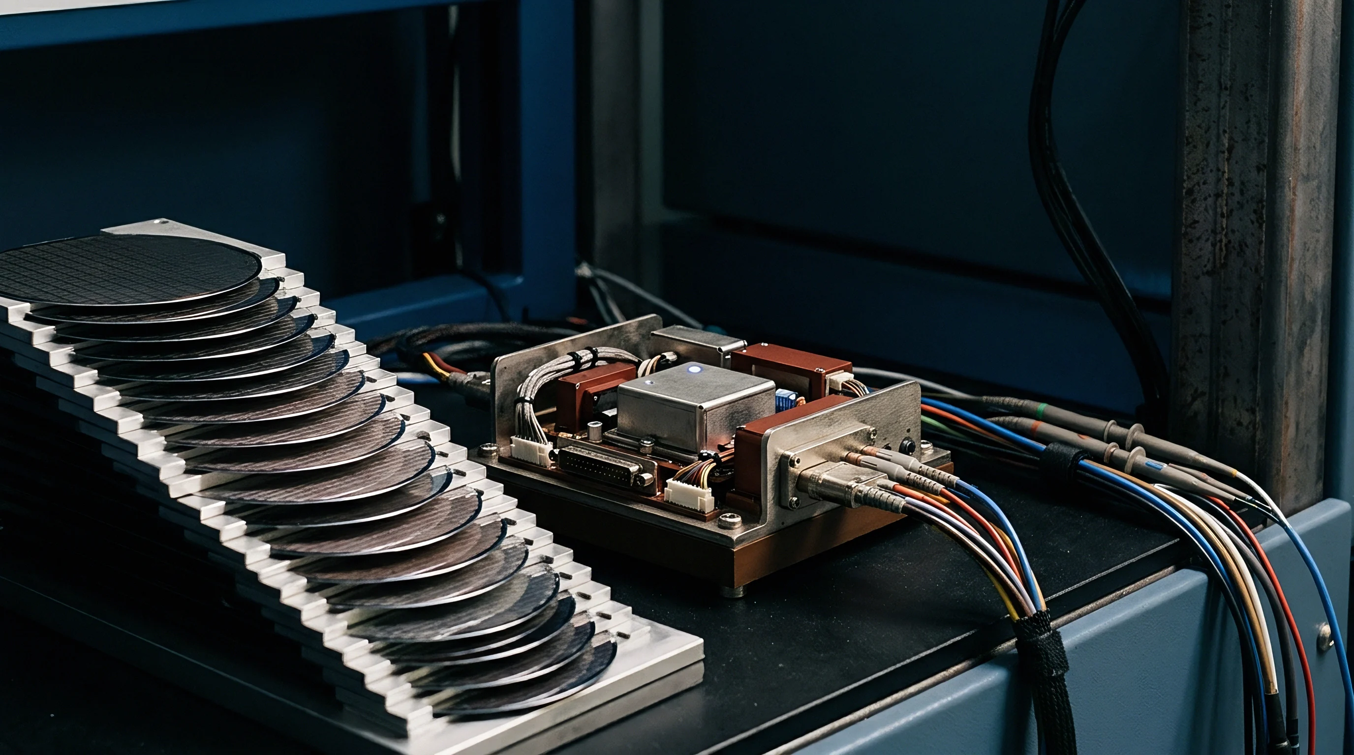
Placing an un-doped polycrystalline silicon layer between the high-resistivity base handle wafer and the buried silicon dioxide layer arrests surface carrier motion. This polycrystalline layer features an extremely high volume of disordered grain boundaries, dangling bonds, and crystallographic dislocations. These structural defects introduce an energetic continuum of deep donor and acceptor states throughout the silicon bandgap, where trap densities within the interfacial zone exceed 10 to the 12th power states per square centimeter electron-volt.

What Prevents Free Carrier Accumulation under High Drive?
Structural defect centers act as rapid capture traps for both electrons and holes, reducing the effective lifetime of free carriers to picosecond regimes and shifting the local dielectric relaxation frequency orders of magnitude above the operating frequency of the front-end module. When fixed oxide charges induce electrostatic potential variations, the mid-gap traps capture the attracted carriers and pin the Fermi level near the intrinsic silicon level. The mobile surface conduction layer fails to form, preserving the high resistivity of the underlying bulk crystal right up to the oxide boundary.
A trap density of 5 times 10 to the 12th states per square centimeter electron-volt preserves substrate resistivity above 2,500 Ohm-centimeters under a 30-volt radio frequency bias.
The thickness of the deposited polycrystalline layer determines its mechanical integrity and electrical buffering capability during subsequent processing steps, with deposition targets sitting between 0.3 and 1.5 micrometers. Layers thinner than 0.3 micrometers risk complete grain consumption during thermal oxidation or device isolation steps. Layers thicker than 1.5 micrometers introduce severe wafer bow due to mechanical tensile stress accumulated during low-pressure chemical vapor deposition, interfering with automated lithographic chucks during front-end-of-line manufacturing.
| Substrate Classification | Effective Surface Resistivity | Trap State Density | Second Harmonic Level | Third Harmonic Level | 5.8 GHz Insertion Loss |
|---|---|---|---|---|---|
| Standard Bulk P-Silicon | 10 Ohm-cm | Below 10^10 cm^-2 eV^-1 | -52 dBc | -58 dBc | 1.25 dB/mm |
| Standard HR-SOI | 45 Ohm-cm | 1.2 x 10^10 cm^-2 eV^-1 | -68 dBc | -72 dBc | 0.42 dB/mm |
| Trap-Rich Poly-Passivated HR-SOI | 2,800 Ohm-cm | 6.4 x 10^12 cm^-2 eV^-1 | -94 dBc | -99 dBc | 0.14 dB/mm |
| Silicon on Sapphire Reference | 10,000 Ohm-cm | Dielectric Insulator | -102 dBc | -106 dBc | 0.08 dB/mm |
Grain boundary densities govern trapping efficiency at elevated temperatures. As operating junction temperatures climb to 105 degrees Celsius inside dense handset packaging, thermal generation rates elevate the density of intrinsic carriers. The trap layer absorbs this excess generation to maintain high substrate impedance under heavy transmission loads.
Interfacial traps control RF leakage far more effectively when grain orientations remain thoroughly randomized across the handle boundary.

Spur
Spectral emissions originating from non-linear substrate interactions create severe operational complications inside modern frequency-division duplexing and carrier aggregation architectures. Third-generation Partnership Project standards mandate transmitter harmonic suppression exceeding -36 dBm or -40 dBm depending on local regional band allocations. In multi-carrier uplinks, the transmitter fundamental mixes with co-existing uplink signals across non-linear substrate channels, causing intermodulation products to drop directly into sensitive receiver bands.
In mobile handsets operating concurrently on LTE Band 3 at 1750 MHz and Band 7 at 2540 MHz, non-linear mixing generates a second-order difference product near 790 MHz, falling squarely into the Band 20 downlink receiver. High-resistivity substrates lacking interfacial trap layers produce intermodulation distortion levels above -85 dBm under dual +20 dBm transmitter drive levels. A trap-rich substrate suppresses these intermodulation products below -115 dBm, preventing receiver desensitization without requiring expensive off-chip diplexers.
ETSI EN 300 328 limits spurious domain emissions above 1 GHz to -30 dBm, driving the rejection requirement for front-end antenna switches.
Evaluating raw module linearity requires disciplined criteria across the entire operating power range:
- Harmonic distortion floor margins define the delta between measured second-harmonic peaks and regional regulatory emission boundaries under worst-case antenna mismatch conditions.
- Intermodulation intercept tracking identifies changes in third-order input intercept points as transmit drive power sweeps between +15 dBm and +32 dBm.
- Isolation integrity under load documents the degradation of unselected switch port isolation when adjacent active ports carry maximum transmit power.
- Cross-modulation transfer ratios quantify the amplitude modulation transfer from an interfering high-power transmission burst onto a weak incoming reception signal.
Field data indicates that a second harmonic reading of -92 dBc at 900 MHz under a +30 dBm drive rests on a trap layer thickness of at least 0.5 micrometers combined with an interface trap density exceeding 3 times 10 to the 12th power per square centimeter electron-volt. That measurement degrades by 8 to 12 dB if the wafer lot undergoes dopant migration during back-end metallization. Sourcing teams verify trap stability by demanding harmonic measurements taken before and after 1,000-hour high-temperature operating life tests, during which unstable lots can see harmonic levels jump by twenty decibels.
| Transmitter Combination | Mixing Product | Impacted Receive Band | Standard Substrate IMD | Trap-Rich Substrate IMD |
|---|---|---|---|---|
| Band 1 (1950 MHz) + Band 3 (1750 MHz) | 2f1 – f2 = 2150 MHz | Band 1 Downlink | -78 dBm | -116 dBm |
| Band 8 (900 MHz) + Band 7 (2500 MHz) | f2 – 2f1 = 700 MHz | Band 28 Downlink | -81 dBm | -118 dBm |
| Band 4 (1710 MHz) + Band 13 (780 MHz) | f1 + f2 = 2490 MHz | Wi-Fi 2.4 GHz Band | -72 dBm | -112 dBm |
| Band 20 (830 MHz) + Band 3 (1750 MHz) | 2f2 – f1 = 2670 MHz | Band 7 Downlink | -76 dBm | -114 dBm |
Whether advanced multi-tier trap engineering can suppress intermodulation products under 50-volt millimeter-wave pulses remains unanswered in commercial foundry PDK documentation.

Drift
Fabrication sequences for modern radio frequency integrated circuits expose the silicon substrate to severe thermal cycles. High-temperature thermal treatments, such as source-drain dopant activation anneals, reach temperatures between 950 and 1050 degrees Celsius. These elevated thermal budgets present severe hazards to the underlying polycrystalline trap microstructure, risking insertion loss penalties that impair overall sensitivity.
Do High Temperature Thermal Cycles Anneal Grain Traps?
Prolonged thermal exposure mobilizes silicon atoms along crystallographic boundaries, triggering solid-phase grain growth. Fine-grained polycrystalline films recrystallize into coarse, large-grained structures with sharply reduced grain boundary surface area per unit volume. In severe cases, the film recrystallizes epitaxially from the underlying monocrystalline handle wafer, eliminating interfacial defect states completely.
Dopants present in adjacent layers diffuse rapidly along boundary pathways, saturating remaining trap states and converting the insulating trap layer into a degenerate semiconductor. Structural metallurgical recrystallization parallels the thermal grain coarsening observed in high-stress aerospace alloys subjected to turbine exhaust heat.
Thermal endurance of passivated trap states requires process budgets restricted beneath equivalent dwell times at elevated processing temperatures.
Foundry teams qualify substrate resilience against thermal degradation through a structured qualification sequence:
- Cleave representative test wafers directly from raw incoming silicon-on-insulator lots prior to active processing.
- Measure baseline substrate harmonic distortion using coplanar waveguide test structures driven at +30 dBm across fundamental bands from 900 MHz to 5 GHz.
- Expose sample wafers to simulated thermal cycles matching the specific time and temperature profiles of active front-end transistor fabrication.
- Extract post-anneal effective resistivity profiles using spreading resistance profiling and high-frequency capacitance-voltage sweeps.
- Reject entire incoming wafer lots displaying effective post-anneal surface resistivity drops exceeding 40 percent of pre-anneal baselines.
Published literature reports post-anneal effective resistivity values ranging from 1,200 to 2,500 Ohm-centimeters for advanced trap-rich wafers, though the upper limit remains unverified under mass-production foundry conditions. Sourcing engineers protect yields by adding thermal endurance guardbands directly into wafer purchase specifications. Proprietary grain-boundary passivation methods aim to prevent thermal degradation during processing, leaving post-processing harmonic degradation to stem from backend metallization stress rather than substrate breakdown.

Premium
Specifying trap-rich high-resistivity silicon-on-insulator substrates adds direct manufacturing costs at the wafer blank level. An engineered 300 mm trap-rich wafer commands a purchase price between 420 and 580 dollars, compared to 280 to 340 dollars for standard high-resistivity silicon-on-insulator material and 90 to 130 dollars for generic bulk silicon. For a 2.5 square millimeter RF switch die, the substrate cost component rises from approximately 1.4 cents on standard silicon to roughly 2.8 cents on certified trap-rich material.
Die-level cost increments are offset by system-level component reductions within the complete front-end module. Eliminating surface conduction harmonics reduces external surface acoustic wave filtering stages and shifts the pass band downward, freeing board area and lowering the overall module bill of materials. The removal of two external harmonic rejection filters saves between 6 and 9 cents in passive component purchases, more than compensating for the die-level silicon surcharge.
| Substrate Category | Raw 300mm Wafer Cost | RF Switch Die Cost (2.5 mm²) | External Filter Cost Required | Total Front-End BOM Cost |
|---|---|---|---|---|
| Bulk Silicon (High Volume) | $110 | $0.009 | $0.140 | $0.420 |
| Standard HR-SOI | $310 | $0.018 | $0.085 | $0.345 |
| Trap-Rich HR-SOI | $495 | $0.028 | $0.000 | $0.275 |
| Gallium Arsenide pHEMT Reference | $1,250 (150mm eq.) | $0.082 | $0.020 | $0.380 |
| Costs reflect typical procurement baselines for high-volume automotive and mobile connectivity modules at 500,000-unit minimum order quantities. | ||||
Commercial purchase contracts governing RF-SOI procurement enforce substrate performance through strict incoming wafer acceptance provisions. Section 4.2 of SEMI M81 establishes standardized test structures and microwave extraction procedures for determining high-frequency substrate loss and harmonic generation. Sourcing agreements incorporating this specific clause bind foundries to credit defective wafer lots whenever second harmonic distortion levels exceed -88 dBc under specified reference probe excitation.