Sub-Threshold Transconductance Modeling for Cryogenic and High Temperature Wireless Timing Architectures
Sub-threshold timing architectures demand dynamic body biasing and fivefold negative resistance margins to prevent clock failure across extreme thermal swings.


Frost
Cryogenic timing architectures in wireless sensor interfaces operate at the edge of weak inversion. At 77 Kelvin liquid nitrogen baselines down to 4 Kelvin liquid helium conditions, the thermal voltage kT/q drops from 25.86 millivolts at room temperature to 6.63 millivolts and 0.34 millivolts respectively. This steep thermal scaling compresses the sub-threshold swing from eighty millivolts per decade to below twenty millivolts per decade in advanced bulk CMOS and fully depleted silicon-on-insulator processes.
The transconductance efficiency gm/Id theoretically spikes toward the thermodynamic limit of q/(n kT), though impurity freeze-out, interface state trapping, and source-drain series resistance intervene long before reaching that boundary on a probe station.
Silicon timing cores for low-power wireless transceivers rely on sub-threshold active devices to sustain oscillation in primary Pierce and complementary cross-coupled topologies. Small-signal transconductance gm dictates whether the core generates enough negative resistance to overcome the equivalent series resistance of the quartz crystal or microelectromechanical resonator. Cooling a 40-nanometer bulk CMOS test die from 300 Kelvin to 77 Kelvin shifts threshold voltage upward by approximately 1.2 millivolts per Kelvin as the Fermi level moves toward the band edges.
A core biased with a fixed sub-threshold current generator starves as gate overdrive vanishes into deep cut-off.
A fixed-voltage gate bias calibrated at room temperature drives sub-threshold timing cores into complete silence below 110 Kelvin.
Measurements on deep sub-micron test vehicles show that the sub-threshold ideality factor n degrades below 100 Kelvin. While room temperature n values hover between 1.15 and 1.30, cryogenic values often exceed 2.20 because interface traps at the silicon-dielectric boundary remain occupied, screening gate control. Effective mobility initially rises from reduced acoustic phonon scattering, peaking around 120 Kelvin, before ionized impurity scattering and surface roughness degrade it at lower temperatures.
The resulting transconductance plateaus instead of tracking inverse temperature linearly.
High-frequency wireless timing synthesis relies on phase-locked loops where the digitally controlled oscillator core consumes under one milliampere. When selecting transceiver silicon for space avionics, quantum readout instrumentation, or superconducting sensor monitoring, designers face severe frequency pulling. Cryogenic operation alters input capacitance in the sub-threshold differential pair, shifting tank resonant frequency upward by two to five percent.
Sourcing teams reviewing vendor qualification data check the cold-start margin under minimum supply rail conditions.
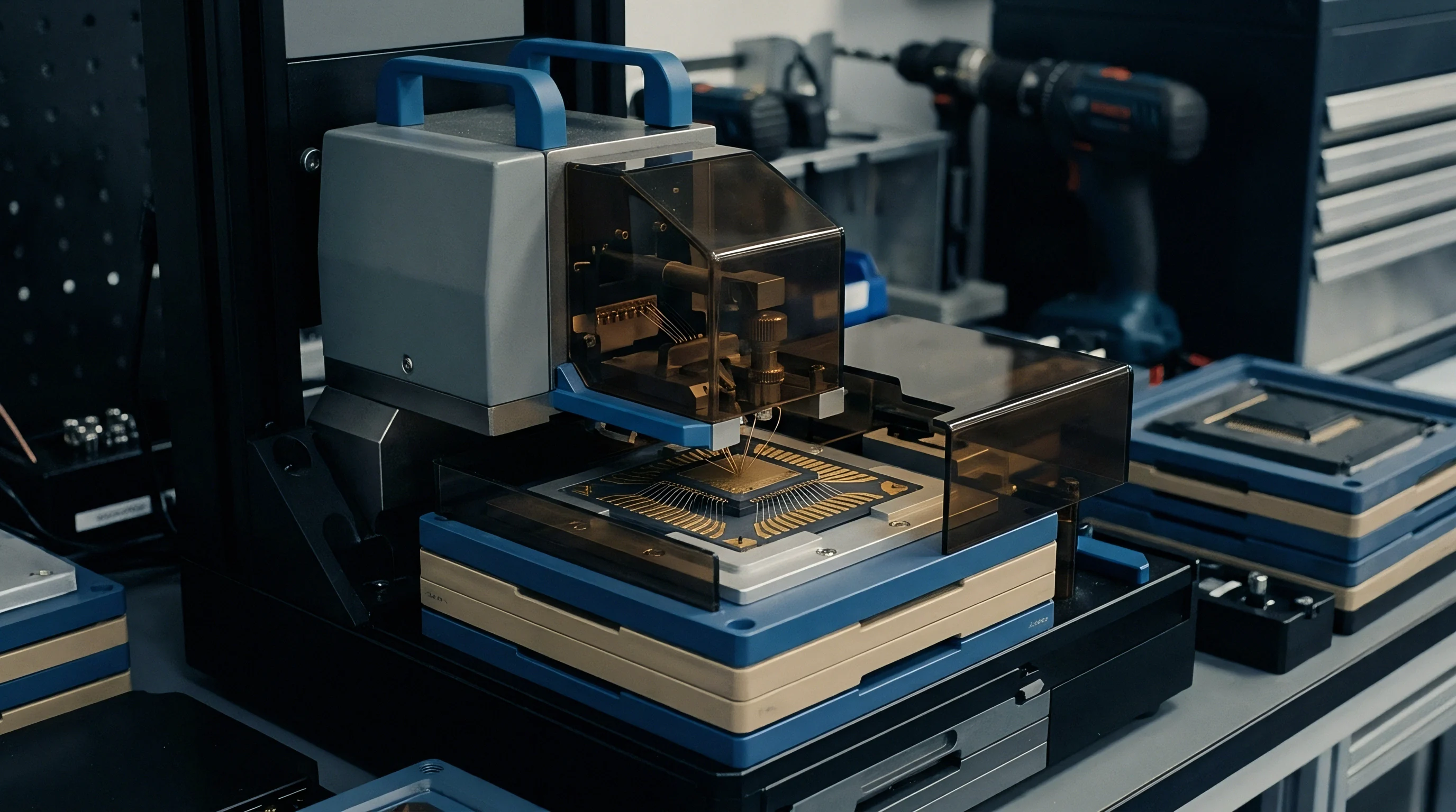
Foundry process design kits rarely provide verified compact models below minus forty degrees Celsius. BSIM4 and BSIM-CMG formulations fail to capture incomplete ionization below 50 Kelvin without empirical patch files. Design houses must extract cryogenic BSIM parameters manually across multiple wafer lots to verify oscillation startup across process corners.
Heat
Downhole telemetry, automotive turbine instrumentation, and industrial furnace monitoring push wireless transceivers toward ambient ceilings of 200 to 300 degrees Celsius. At 573 Kelvin, thermal voltage reaches 49.38 millivolts. The sub-threshold slope broadens severely, surpassing 180 millivolts per decade in standard bulk silicon.
Sub-threshold transconductance efficiency gm/Id collapses as the channel loses electrostatic confinement, pushing the device out of weak inversion into a drift-dominated moderate conduction regime at microampere bias points.
Reverse-biased pn junction leakage escalates exponentially with temperature, doubling roughly every eight to ten degrees Celsius in unhardened planar CMOS. At 250 degrees Celsius, parasitic junction leakage currents swamp the sub-threshold operating current of low-power reference oscillators. A 32.768 kilohertz real-time clock oscillator designed for a fifty-nanoampere core bias sees junction leakage exceed one microampere.
The active core stops acting as a controlled negative conductance generator, degrading phase noise and stopping the clock.
Junction leakage across unhardened bulk silicon destroys sub-threshold negative resistance above 225 degrees Celsius.
Silicon-on-insulator technology mitigates junction leakage by isolating active islands above a buried oxide layer, slashing leakage volume by three orders of magnitude. However, thin silicon film introduces high-temperature back-channel conduction if substrate bias remains unmanaged. Wide-bandgap alternatives ~ notably silicon carbide and gallium nitride ~ push sub-threshold limits beyond 400 degrees Celsius, though integration with dense digital basebands remains commercially constrained.
Silicon carbide junction field-effect transistors provide stable transconductance profiles across extreme heat, but lacking complementary p-channel devices complicates oscillator loop synthesis.
Threshold voltage drops linearly as temperature climbs, falling at negative 1.5 to negative 2.5 millivolts per Kelvin. While this shift lowers the gate-to-source voltage needed for conduction, simultaneous mobility degradation from intense lattice scattering suppresses transconductance gain. A timing cell optimized for room temperature sub-threshold operation drifts into a state of diminished transconductance and excessive substrate loss, widening loop phase jitter.


Oscillation
Oscillator startup relies entirely on small-signal transconductance overcoming the combined losses of the resonator tank and interconnects. Barkhausen criteria define the boundary where loop gain magnitude equals unity with zero net phase shift around the feedback path. In a standard Pierce oscillator circuit, effective negative resistance delivered by the sustaining active stage equals transconductance divided by the product of the two load capacitances and the square of oscillation angular frequency.
Temperature excursions alter every variable in this negative resistance relation at once. At low temperatures, quartz resonator equivalent series resistance spikes from internal friction peaks and package gas condensation. At elevated temperatures, quartz acoustic losses climb steadily, raising motional resistance from a baseline of thirty ohms up to several hundred ohms.
The sub-threshold active stage must supply sufficient transconductance across this entire trajectory.
| Operating Temperature (K) | Thermal Voltage (mV) | Sub-Threshold Swing (mV/dec) | Peak gm/Id (1/V) | Motional ESR (Ohms) | Startup Margin Ratio |
|---|---|---|---|---|---|
| 4.2 | 0.36 | 14.2 | 48.5 | 320 | 1.8 |
| 77.0 | 6.63 | 28.5 | 29.2 | 85 | 4.6 |
| 300.0 | 25.86 | 78.0 | 26.4 | 35 | 5.2 |
| 450.0 | 38.78 | 124.0 | 15.8 | 110 | 2.9 |
| 573.0 | 49.38 | 182.0 | 8.4 | 280 | 1.1 |
A rigorous startup condition demands an oscillation allowance ratio of at least three under nominal operating targets, expanding to five for high-reliability industrial and orbital deployments. This ratio compares small-signal negative resistance to the maximum equivalent series resistance of the crystal. If negative resistance falls below three times the resonator resistance, random thermal fluctuations will not build into stable limit-cycle oscillations within protocol slot timing budgets.
Are Bias Generators Capable of Stabilizing Loop Transconductance?
Constant transconductance bias networks attempt to track temperature shifts by referencing core currents to thermal voltages or internal resistors. Standard architectures tie the active device gate voltage to a proportional-to-absolute-temperature current generator. This tracking fails at cryogenic baselines where carrier freeze-out alters resistor sheet resistance, turning a planned constant transconductance state into runaway bias and stalling the circuit.
At high temperatures, proportional-to-absolute-temperature currents increase channel inversion, pulling the transistor out of sub-threshold into saturation. Power consumption multiplies fivefold, collapsing the power budget as battery reserves empty prematurely. Dynamic body biasing offers a corrective path by shifting local substrate potential to clamp threshold voltage against thermal drift.
- Proportional Current Tracking establishes stable loop gain across standard industrial ranges, but introduces severe channel inversion errors above 200 degrees Celsius.
- Adaptive Well Biasing compensates threshold voltage fluctuations through closed-loop back-gate charge injection across wide thermal spans.
- Switched Capacitor Degeneration suppresses excess low-temperature transconductance to prevent mechanical resonator overdrive and quartz fracture.
- Fractional Bandgap Generation supplies stable microvolt-level gate references down to cryogenic floors without relying on uncalibrated diffusion resistors.
Resonator overdrive poses an equal risk at cryogenic temperatures. When transconductance jumps from elevated low-field mobility, drive levels delivered to the quartz blank can exceed two microwatts. This induces nonlinear quartz elasticity, frequency hops, and physical electrode delamination over thermal cycling.

Sourcing
Module procurement for extreme-environment wireless hardware exposes severe disconnects between silicon ratings and real assembly tolerances. Standard off-the-shelf transceiver modules specified for industrial bands between minus forty and plus eighty-five degrees Celsius incorporate components that fail immediately outside those bounds. Crystal unit hermeticity, solder alloy composition, substrate glass transition temperatures, and passive component dielectric integrity dictate survival.
Standard tin-lead or lead-free SAC305 solder interconnections undergo phase transformations and embrittlement below minus fifty degrees Celsius, cracking under thermal shock. High-temperature designs require specialized gold-tin or high-lead solders alongside high-melting-point polyimide or ceramic low-temperature co-fired ceramic module substrates. Sourcing specifications mandate rigorous environmental stress screening protocols before delivery sign-off.
| Regime | Silicon Process | Substrate Material | Interconnect Metallurgy | Relative Module Cost Multiplier |
|---|---|---|---|---|
| Cryogenic (4K – 77K) | 28nm FD-SOI | Ceramic LTCC | Gold-Indium Solders | 4.5x |
| Industrial (-40C – 85C) | 40nm Bulk CMOS | FR4 High-Tg | Standard SAC305 | 1.0x |
| Automotive (-40C – 125C) | 65nm Automotive CMOS | Polyimide Flex | SAC405 with Doping | 1.4x |
| Harsh (-55C – 175C) | 180nm SOI | High-Tg Polyimide | High-Lead PB90 | 2.8x |
| Geothermal (Up to 300C) | SiC / Custom SOI | Alumina / AlN Ceramic | Au-Sn Eutectic | 8.2x |
Procurement contracts require distinct environmental validation matrices. Component screening documents define acceptance sampling across thermal shock chambers, liquid nitrogen immersion, and sustained high-heat soaking. Sourcing engineers review qualification dossiers to verify whether transconductance drift margins have been characterized through lot-specific wafer acceptance tests.
- Lot Acceptance Screening mandates cryogenic probe testing of wafer drop-in test structures to weed out lots exhibiting excessive interface trap density.
- Package Seal Verification confirms hermetic cavity leak rates comply with military standards to prevent moisture condensation during rapid temperature swings.
- Acoustic Wave Qualification tracks resonator motional parameters inside high-temperature soak chambers across one thousand operating hours.
- Interconnect Shear Testing inspects the physical resilience of gold wirebonds against thermal fatigue and intermetallic compound formation.
Second-sourcing extreme-temperature timing modules introduces severe friction. Commercial transceiver pinouts rarely match between specialized foundries, locking the bill of materials into single-source dependencies. Contract negotiations focus on long-term silicon die bank storage and multi-year supply guarantees to protect against unexpected fab retirements.
A contract omitting lot-specific cryo-soak validation leaves the buyer footing the scrap bill when standard foundry corners freeze out.
Testing completed modules at liquid helium or downhole temperatures multiplies test costs. Specialized automated test equipment equipped with thermal stream heads and vacuum cryostats carries high hourly rates. Buyers must evaluate whether a vendor performs full-temperature functional testing or relies on guard-banded room-temperature vector extrapolation.

Protocol
Wireless standards depend strictly on physical layer symbol timing, packet synchronization, and channel carrier spacing. Oscillator frequency drift induced by transconductance-dependent load pulling directly degrades radio link budgets. When transconductance drops, the active stage induces excess phase delay across the sustaining feedback network, pulling the oscillation frequency away from its nominal series resonance point and shifting radio transmissions outside the assigned channel raster.
In low-power wide-area systems operating on sub-gigahertz allocations, such as LoRa deployments at 868 megahertz or 915 megahertz, transceiver frequency errors degrade demodulation sensitivity. A 125 kilohertz bandwidth LoRa signal tolerates a maximum offset of twenty-five percent of the channel bandwidth ~ thirty-one kilohertz of allowable error across transmitter and receiver combined. At 915 megahertz, this budget corresponds to an aggregate reference clock tolerance of thirty-four parts per million.
| Protocol Standard | Nominal Band | Clock Tolerance (ppm) | Sleep Drift Impact | Link Margin Degradation |
|---|---|---|---|---|
| LoRaWAN Spreading Factor 12 | 868 / 915 MHz | ±30 | RX Window Misalignment | 3.5 dB Sensitivity Loss |
| Bluetooth Low Energy 2 Mbps | 2.4 GHz ISM | ±50 | Connection Window Drift | Packet Drop Rate Spikes |
| IEEE 802.15.4 DSSS | 2.4 GHz ISM | ±40 | Symbol Clock Slipping | 2.0 dB EVM Penalty |
| Narrowband IoT Cat-NB1 | Sub-1 GHz Bands | ±20 | Subcarrier Sync Loss | Complete RRC Disconnect |
Clock drift devastates sleep-wake scheduling in synchronized mesh and cellular low-power regimes. In Bluetooth Low Energy implementations, connection intervals dictate that peripheral nodes wake precisely inside scheduled anchor points. A 32.768 kilohertz sleep clock experiencing transconductance starvation drifts by several hundred parts per million over temperature swings, causing the peripheral to miss the central master packet.
The peripheral re-enables its receiver early to compensate, lengthening the listen window and draining microampere reserves.
At elevated temperatures, degraded transconductance efficiency combined with crystal ESR escalation delays oscillator startup from hundreds of microseconds to tens of milliseconds. In a battery-operated sensor transmitting once per minute, startup airtime overhead dominates total energy consumption. If startup current flows for thirty milliseconds instead of one millisecond, product service life contracts from ten years down to eighteen months.
Regulatory frameworks across international jurisdictions strictly police out-of-band emissions. The Federal Communications Commission and the European Telecommunications Standards Institute enforce steep spectrum emission masks on unlicensed industrial, scientific, and medical bands. A timing cell whose transconductance pulls carrier frequency across temperature boundaries violates band edges, risking customs seizures and revocation of equipment authorizations.
Selecting transceiver architecture for extreme environments balances physical link range against timing stability. In high-temperature subterranean deployments, spreading factors must contract to widen receiver tracking loops, sacrificing receiver sensitivity to accommodate crystal pulling. This protocol concession drops the available link budget by three to six decibels, halving transmission distance through geological strata.
Passive temperature compensation software cannot resolve physical timing errors when transconductance starvation halts the crystal entirely. Software algorithms cannot calibrate an oscillator that fails to oscillate. Hardware specifications govern radio link viability.