Verifying Sliding Window Time Bucket Synchronization across Unpowered Sleep Cycles without Backup Real-Time Clocks
Verify crystal-less sleep synchronization by combining dynamic polynomial thermal compensation with scaled receiver guard windows to maintain sliding time buckets safely.

Phase
An edge node drawing 120 nanoamperes in shut-down mode reaches that floor by cutting main rail power to all crystal oscillators. Omitting the 32.768 kHz quartz crystal saves six cents in bill-of-materials cost and four square millimeters of board space, but absolute timekeeping stops the microsecond the power gate opens. The micro-controller retains state through ultra-low-leakage static RAM, while elapsed time in off states is estimated by an internal low-speed RC oscillator or an analog resistor-capacitor decay circuit.
These internal RC clocks drift between 20,000 and 50,000 parts per million across the industrial operating temperature band. A 30-minute sleep cycle with 3 percent clock drift introduces 54 seconds of absolute timing uncertainty, throwing off sliding window time bucket synchronization between telemetry endpoints and host aggregation nodes.
Sliding window time buckets split continuous telemetry data into discrete, rolling temporal blocks. Smart water meters, distribution line monitors, and cold-chain sensors aggregate readings into uniform intervals, such as 15-minute energy calculations, 60-second peak flow rates, or rolling 24-hour transmission caps required by telecommunications regulators. Without a shared real-time clock reference, multiple battery-powered endpoints reporting to a single receiver will drift out of step.
The base station expects timestamps to match its own high-precision atomic or satellite-derived clock. If an endpoint timer runs slow and generates a packet at second 899 of a 900-second window, that frame can land in second 15 of the subsequent window at the host server, corrupting billing records, rate-limiting calculations, and duty-cycle logs.
Oscillator Dynamics in Shut-Down Modes
Silicon architectures for battery-operated wireless nodes divide power delivery into separate power domains. The core logic domain runs the main processor, system bus, and high-speed system clock source ~ typically a 16 MHz to 32 MHz quartz crystal oscillator. The ultra-low-power sleep domain holds retention memory, reset circuitry, watchdog timer, and low-speed sleep clock.
To push deep sleep current figures below 500 nanoamperes, architects power down the high-speed crystal driver completely. High-speed quartz crystals take hundreds of microseconds and several microjoules of energy just to stabilize oscillation upon wake-up. Running an external 32.768 kHz tuning-fork quartz crystal during sleep keeps frequency drift down to 20 parts per million, but the oscillator inverter circuit draws a constant 600 to 900 nanoamperes from the battery cell.
Removing that low-speed crystal forces the sleep domain to rely on an integrated silicon low-speed RC oscillator.
Integrated RC oscillators operate by charging and discharging integrated capacitor arrays using internal current sources. Operational frequency shifts directly with junction temperature, supply voltage, and silicon process variations. Silicon vendors specify low-speed RC accuracy at a baseline 25 degrees Celsius and a fixed 3.0-volt supply, where frequency error stays within plus or minus 1 percent.
But in the field, ambient temperatures can swing from minus 40 degrees Celsius in an unheated enclosure up to 85 degrees Celsius under direct solar exposure, causing internal charge currents to change exponentially. Silicon mobility drops, threshold voltages shift, and the nominal 32.768 kHz RC clock frequency wanders between 28 kHz and 36 kHz. The table below outlines how clock source choices alter power performance and temporal drift across low-power operational states.
| Clock Source Type | Typical Sleep Current | Frequency Drift (-40C to +85C) | Sleep Duration Error per Hour | Startup Latency |
|---|---|---|---|---|
| External 32.768 kHz Tuning Fork Quartz | 650 nA to 1200 nA | +/- 20 ppm to +/- 150 ppm | 0.072 seconds to 0.54 seconds | 1000 us to 3000 us |
| Internal Ultra-Low-Power RC (LSI) | 30 nA to 120 nA | +/- 20,000 ppm to +/- 50,000 ppm | 72.0 seconds to 180.0 seconds | 2 us to 10 us |
| Factory-Calibrated High-Speed RC (HSI/1024) | 15 uA to 45 uA | +/- 5,000 ppm to +/- 15,000 ppm | 18.0 seconds to 54.0 seconds | 1 us to 5 us |
| External Temperature-Compensated TCXO (32.768 kHz) | 1500 nA to 3500 nA | +/- 2 ppm to +/- 5 ppm | 0.007 seconds to 0.018 seconds | 500 us to 1500 us |
Unpowered sleep cycles compound these timing errors because the micro-controller loses its counter state during power-down transitions. When the system shuts down, the main hardware counter stops. The micro-controller saves its current sliding window state into retention RAM, enables the low-power RC wake-up timer, and sets the main voltage regulator to low-power bypass mode.
Throughout sleep, the node has no reference for absolute physical time. When the low-power timer fires its wake-up interrupt, the core power domain re-arms, the high-speed crystal starts up, and software attempts to reconstruct the true timestamp. Calculated sleep duration equals the requested count multiplied by the nominal RC clock period, adjusted by an estimated drift factor.
But because environmental shifts alter drift dynamically during sleep, the reconstructed timestamp diverges from true wall-clock time.
Unpowered sleep cycles without quartz references transform absolute time registers into probabilistic software estimates.
Sliding Bucket Misalignment Mechanics
Sliding window algorithms calculate metrics across moving temporal ranges, advancing continuously or stepping at precise sub-intervals. Consider a sub-GHz utility monitoring node that aggregates water flow data into 15-minute sliding buckets, updating its local histogram every 60 seconds. The endpoint relies on these sliding buckets to stay within regional wireless transmission limits, such as European Telecommunications Standards Institute rules capping sub-GHz duty cycles at 1 percent per hour in the 868 MHz ISM band.
If the endpoint clock drifts by 4 percent over an extended off-cycle, the local 1-hour rolling window counter inside the device steps out of sync with the regulator’s receiver window.
Accumulated timing phase error corrupts data alignment across multiple operational layers. This failure mode shows up during field evaluations of unpowered sensor nodes deployed on industrial pipelines. The system architecture depends on aligned sliding time buckets to achieve predictable operation across four distinct layers:
- Data Aggregation Buckets accumulate sensor readings into deterministic time slots, such as 15-minute energy totals. Misaligned endpoints place sensor samples into wrong time intervals, producing artificially skewed peak-demand metrics at the central server.
- Radio Receiver Slot Alignment mandates that the endpoint wakes up exactly when the host gateway opens its reception window. Phase error causes the endpoint to wake up after the gateway finishes receiving, resulting in complete transmission loss.
- Regulatory Duty-Cycle Tracking enforces sliding hourly transmit caps across shared sub-GHz spectrum. Clock acceleration causes an endpoint to exhaust its permitted airtime allowance prematurely inside a host regulator’s window, triggering software lockouts.
- Energy Storage Management balances battery discharge profiles by pacing transmission bursts over rolling windows. Clock skew compresses multiple transmission bursts into a narrow true-time window, pulling heavy peak currents that drop internal cell voltage.
Phase divergence grows linearly with sleep duration and non-linearly with environmental thermal gradients. An endpoint sleeping for 60 seconds experiences minimal drift, rendering internal RC clock errors manageable. But an endpoint sleeping for 12 hours between reporting cycles accumulates tens of minutes of drift.
When it wakes to check whether a sliding bucket boundary has passed, its local software clock may indicate that 12 hours have elapsed, whereas absolute ground-truth time shows 11 hours and 38 minutes. If the endpoint transmits its payload tagged with that software timestamp, the receiver rejects the frame as a duplicate or drops it outside the active database sliding window. Hardware developers must quantify this clock drift before selecting a crystal-less micro-controller architecture.
How far an endpoint can drift before its sliding window synchronization breaks down entirely depends on protocol tolerance and guard window design.
Anchor
Wireless link protocols correct for hardware clock drift by using host anchor frames transmitted by mains-powered gateways, base stations, or central access points. Protocols like LoRaWAN Class B, Bluetooth Low Energy synchronized advertising streams, IEEE 802.15.4 Time-Synchronized Channel Hopping, and Cellular NB-IoT Extended Discontinuous Reception rely on these periodic transmission anchors. The gateway broadcasts a high-precision timestamp frame derived from an onboard satellite receiver or atomic clock.
When a battery-powered endpoint wakes up, it listens for this anchor frame, measures the difference between expected arrival time and actual reception time, and calculates its temporal offset. Firmware then uses this offset to realign local sliding window bucket indices to ground-truth time.
Re-synchronization comes at a measurable RF airtime cost. When an endpoint lacks a precise local clock reference, it cannot predict the exact microsecond an anchor frame will arrive over the air. To avoid missing an anchor frame that arrived early due to clock acceleration, the endpoint opens its radio receiver in advance of the nominal window start time.
This early opening forms a guard window. The width of the guard window scales directly with maximum anticipated clock drift accrued since the last valid anchor frame reception. Widening the guard window keeps the link reliable, but forces the radio receiver to run idle while waiting for the preamble.
This idle receiver current drains the battery cell far faster than short sensor sampling routines.
Gateway Timing Headers and Protocol Frames
Each wireless protocol implements anchor timing through distinct frame formats and MAC layer mechanisms. In sub-GHz LoRaWAN Class B networks, gateways broadcast a beacon frame every 128 seconds. The beacon payload carries a GPS-aligned epoch timestamp alongside network timing parameters.
Endpoints use this beacon to synchronize their internal ping-slot schedules, allowing incoming downlink frames to land in tight 30-millisecond reception windows. When an endpoint operates without a backup quartz crystal, sleeping for the full 128-second beacon period without thermal tracking drifts the local clock beyond the default receiver window, requiring extensive software guard bands.
In IEEE 802.15.4 TSCH link topologies, nodes exchange Enhanced Beacons that specify absolute slotframe numbers and offset times. Channel hopping schedules depend on absolute frame synchronization across hundreds of sequential time slots, each typically 10 milliseconds wide. A clock offset exceeding 1 millisecond shifts the transmission out of the slot center, causing packet collisions or total receiver miss.
Cellular LTE-M and NB-IoT nodes operating in deep power-saving modes align their wake cycles to System Information Block broadcasts from eNodeB towers. The eNodeB maintains absolute network timing, providing a baseline reference whenever user equipment exits power-saving modes. The receiver parameters for major wireless protocols operating without backup RTC sources are detailed in the table below.
| Protocol Standard | Nominal Anchor Interval | Native Receiver Slot Width | Max Permitted Drift Without Miss | Guard Window Penalty at 3% Drift |
|---|---|---|---|---|
| LoRaWAN Class B (Beacon) | 128 seconds | 30 ms | +/- 15 ms | 7.68 seconds |
| IEEE 802.15.4 TSCH | 1.0 to 10.0 seconds | 10 ms | +/- 1.0 ms | 0.30 seconds |
| BLE Periodic Advertising (PAwR) | 0.1 to 2.5 seconds | 1.25 ms | +/- 0.25 ms | 0.075 seconds |
| Cellular NB-IoT (eDRX) | 20.48 to 1048.57 seconds | 10 ms | +/- 5.0 ms | 31.45 seconds |
Calculating the required guard window width relies on a linear drift model based on elapsed sleep time and maximum bounds of silicon variation. Equation 1 defines the minimum guard window duration required to reliably capture an incoming anchor frame:
Guard Window = 2 (Sleep Duration (Drift RC + Drift Temp + Drift Aging)) + Preamble Length + Turn-on Latency
Where Drift RC represents baseline internal RC oscillator tolerance, Drift Temp models temperature-induced frequency shifts, and Drift Aging accounts for semiconductor silicon degradation over multi-year field lifespans. If an endpoint sleeps for 300 seconds using an internal RC oscillator with a combined drift coefficient of 30,000 parts per million (3 percent), the worst-case timing offset equals plus or minus 9 seconds. The endpoint opens its receiver 9 seconds before the scheduled anchor arrival time and holds it open for up to 18 seconds total.
At an active receiver current of 11 milliamperes, an 18-second receiver window consumes 198 millicoulombs of charge per wake cycle, neutralizing the power advantages achieved by using unpowered sleep modes.
Widening the RF receiver guard window guarantees frame capture at the direct expense of battery service life.
Guard Window Expansion and Energy Cost
The energy budget of a crystal-less wireless endpoint is governed by the ratio of receiver guard window power to active processing power. A node equipped with an external 20 ppm crystal sleeping for 300 seconds incurs a clock drift of only 6 milliseconds. Its guard window opens just 6 milliseconds early, consuming negligible active receiver charge.
The crystal-less node sleeping for the same 300 seconds spends orders of magnitude more energy holding its receiver open to catch the same anchor frame.
This airtime energy penalty breaks down into specific phase components during every anchor acquisition cycle:
- System Wake and Crystal Stabilization Phase turns on the internal high-speed system oscillator, restores core power rails, and reloads micro-controller context from RAM.
- RF Transceiver Warm-Up Phase initializes phase-locked loops, powers up low-noise amplifiers, and tunes the synthesizer to the operational channel frequency.
- Guard Window Idle Receive Phase holds the receiver in active search mode prior to frame preamble detection, absorbing baseline thermal clock skew.
- Preamble Detection and Frame Sync Phase locks onto incoming packet headers, processes MAC timing frames, and extracts the host clock reference.
- Timestamp Adjustment and Sleep Calculation Phase updates local software sliding bucket registers, recalculates drift rates, and programs the sleep timer for the next cycle.
Data frames landing inside sliding time buckets require verifiable timestamps. When an endpoint catches a gateway anchor frame, it recalibrates its internal low-speed RC oscillator against the exact arrival time of the host payload. Software calculates the actual number of system clock ticks elapsed between consecutive anchor frames, compares that count against theoretical ticks for an ideal 32.768 kHz reference, and updates a dynamic clock scale factor.
This clock scale factor corrects short-term sleep calculations. If ambient temperature shifts rapidly while the endpoint sleeps, the pre-calculated scale factor fails to prevent temporal misalignment, forcing further guard window expansion.
Anchor frames must arrive on predictable schedules or the link budget defaults to continuous active search mode.
Thermal
Software-driven compensation algorithms correct RC clock drift by mapping micro-controller temperature measurements to oscillator frequency response curves. Modern low-power micro-controllers feature internal silicon temperature sensors connected to analog-to-digital converters, accessible even during brief periodic wakeups. Because internal RC oscillator drift follows deterministic thermal laws governed by silicon bandgap behavior, software compensation polynomials predict frequency variations across temperature shifts without using external quartz references.
The core compensation loop executes directly before entering and immediately after exiting an unpowered sleep cycle. Before power-down, the micro-controller samples its internal temperature sensor, evaluates the temperature-to-frequency polynomial equation, and converts desired sleep duration into an adjusted count of RC clock ticks. If temperature changes rapidly during deep sleep, the pre-sleep adjustment value accumulates phase error.
To resolve this, multi-stage compensation schemes sample temperature during short intermediate wakeups, dynamically adjusting the sleep counter to keep sliding window bucket edges aligned to absolute time references.

Polynomial Frequency Compensation Curves
The mathematical representation of RC oscillator drift across temperature combines second-order and third-order polynomial functions. Equation 2 expresses the normalized frequency offset of an internal RC clock as a function of ambient temperature:
Frequency Offset = A (T – T0)^2 + B (T – T0) + C
Where T represents measured junction temperature, T0 represents factory calibration temperature (typically 25 degrees Celsius), and coefficients A, B, and C are calibration constants stored in micro-controller non-volatile flash memory during manufacturing testing. Parameter C captures baseline initial accuracy offset, parameter B corrects for linear thermal drift, and parameter A models parabolic curvature caused by semiconductor mobility changes at thermal extremes.
Factory calibration procedures measure internal RC oscillator frequency across two known test temperatures, usually 25 degrees Celsius and 70 degrees Celsius, writing the resulting offset values into secure device configuration pages. During field operation, the node reads these parameters to execute polynomial correction calculations. The empirical drift data shown in the table below comes from thermal chamber tests of unpowered micro-controllers, evaluating raw RC drift against polynomial-compensated performance.
| Test Temperature (C) | Uncompensated Frequency Shift | Polynomial Corrected Offset | Residual Drift (ppm) | Max Bucket Error per 24 Hours |
|---|---|---|---|---|
| -40.0 C | -3.85 % (-38,500 ppm) | +0.08 % (+800 ppm) | 800 ppm | 69.12 seconds |
| -10.0 C | -1.42 % (-14,200 ppm) | +0.02 % (+200 ppm) | 200 ppm | 17.28 seconds |
| +25.0 C (Baseline) | +0.05 % (+500 ppm) | +0.005 % (+50 ppm) | 50 ppm | 4.32 seconds |
| +60.0 C | +1.85 % (+18,500 ppm) | -0.03 % (-300 ppm) | 300 ppm | 25.92 seconds |
| +85.0 C | +4.20 % (+42,000 ppm) | -0.09 % (-900 ppm) | 900 ppm | 77.76 seconds |
Polynomial compensation slashes uncompensated drift from 42,000 parts per million down to under 1,000 parts per million across the industrial operating band. This improvement allows system software to narrow receiver guard windows significantly, cutting energy consumption during anchor frame acquisition cycles. Residual drift persists due to non-linear thermal hysteresis, quantization limits in internal temperature sensors, and self-heating effects that occur when the processor wakes to take thermal readings.
Polynomial thermal compensation cuts raw RC oscillator drift by up to forty-fold, shrinking RF receiver guard windows down to millisecond scales.
Can Software Polynomials Eliminate Hardware Crystals Entirely?
Eliminating external crystals depends on whether maximum residual drift satisfies protocol timing budgets across the system’s operational temperature limits. In low-duty-cycle telemetry deployments where endpoints sleep for 15 to 60 minutes and communicate via wide receive windows, polynomial-compensated RC timing provides sufficient temporal alignment to keep sliding buckets organized. In high-density time-synchronized link architectures like TSCH or high-throughput BLE audio streams, residual RC drift of 800 ppm introduces over 48 milliseconds of offset per minute, exceeding standard slot boundaries and causing link failures unless anchor frames arrive every few seconds.
Rapid thermal transients introduce failure modes that static polynomial models cannot correct. When an outdoor asset monitor moves from a heated warehouse into sub-zero winter temperatures, thermal gradients across the silicon substrate create time-lag errors between the internal temperature sensor diode and the RC clock circuit. The sensor measures a higher temperature than the oscillator core actually experiences, causing the polynomial equation to calculate incorrect frequency compensation factors.
To mitigate transient thermal skew, firmware developer suites implement dynamic temperature rate-of-change tracking:
- Temperature Derivative Calculation computes the thermal slope between consecutive wake cycles, flagging rapid temperature transitions.
- Adaptive Wake Scheduling increases intermediate wake-up frequency when thermal derivatives exceed predefined thresholds, preventing phase error accumulation.
- Guard Band Scaling automatically expands receiver window width during thermal transients to prevent missed anchor frames.
- Polynomial Gain Adjustment updates compensation coefficients dynamically when anchor frame timestamps arrive from host infrastructure.
Supply Voltage Sensitivity and Aging Effects
Internal RC oscillator frequency varies with supply voltage delivered by discharging lithium battery chemistry. As a primary thionyl chloride or manganese dioxide battery cell drains from 3.6 volts down to its 2.0-volt cut-off threshold, internal reference currents shift, altering RC oscillator charging periods. Micro-controllers without dedicated internal low-dropout voltage regulators supplying the low-power domain suffer severe voltage-induced clock drift, adding up to 5,000 parts per million of frequency shift per volt of supply drop.
Integrating supply voltage measurement into the compensation loop eliminates this variable. Firmware measures the internal analog voltage rail during active wake cycles alongside temperature readings. A multi-variable lookup table or two-dimensional surface polynomial calculates frequency correction factors based on both voltage and temperature inputs.
Over multi-year deployment lifespans, silicon aging effects alter internal resistor values and dielectric constants inside integrated capacitors, drifting baseline calibration parameters. Network designs correct for multi-year aging drift by using network timing anchors to continuously recalibrate baseline polynomials over the air.
Field trials lost three weeks of test data because uncompensated voltage drops under cold thermal loads skewed local clock registers beyond the recovery limit of host server windows.
Probe
Verifying crystal-less sliding window synchronization requires test setups capable of measuring sub-microamp current profiles alongside high-speed digital radio frames across wide thermal bands. Standard lab oscilloscopes lack the dynamic range to measure nanoampere sleep currents and multi-milliampere transmit spikes simultaneously without saturating amplifiers. Engineers use specialized current profiling hardware, such as auto-ranging power analyzers or precision current probes, synchronized with multi-channel logic analyzers and programmable RF attenuators.
The bench verification setup monitors three synchronous signals: micro-controller sleep power draw, digital General Purpose Input/Output pins toggled at sliding window bucket boundaries, and RF transmission packets captured by a calibrated sniffer receiver. The test environment places the device under test inside a programmable environmental chamber capable of sweeping temperatures from minus 40 degrees Celsius to plus 85 degrees Celsius at controlled ramp rates. This physical setup tracks phase drift accumulation across simulated multi-day deployment profiles.
Bench Profiling Infrastructure and Triggering Setup
Constructing a repeatable test setup requires isolated ground planes, shielded RF enclosures, and low-noise power sources to avoid introducing external interference into sensitive low-power measurements. Mains-powered bench supplies introduce high-frequency switching noise that distorts nanoampere sleep measurements. Specialized battery simulators or linear low-noise power supplies supply clean DC voltage to the target board, matching real battery output impedance.
The micro-controller firmware is configured to output hardware trigger pulses on dedicated test points. A pulse fires when the device enters deep power-down sleep, a second pulse fires when the internal sleep timer triggers a wake-up event, and a third pulse toggles when RF preamble transmission begins. A logic analyzer samples these trigger signals at 100 megasamples per second, providing 10-nanosecond timing resolution across extended test runs.
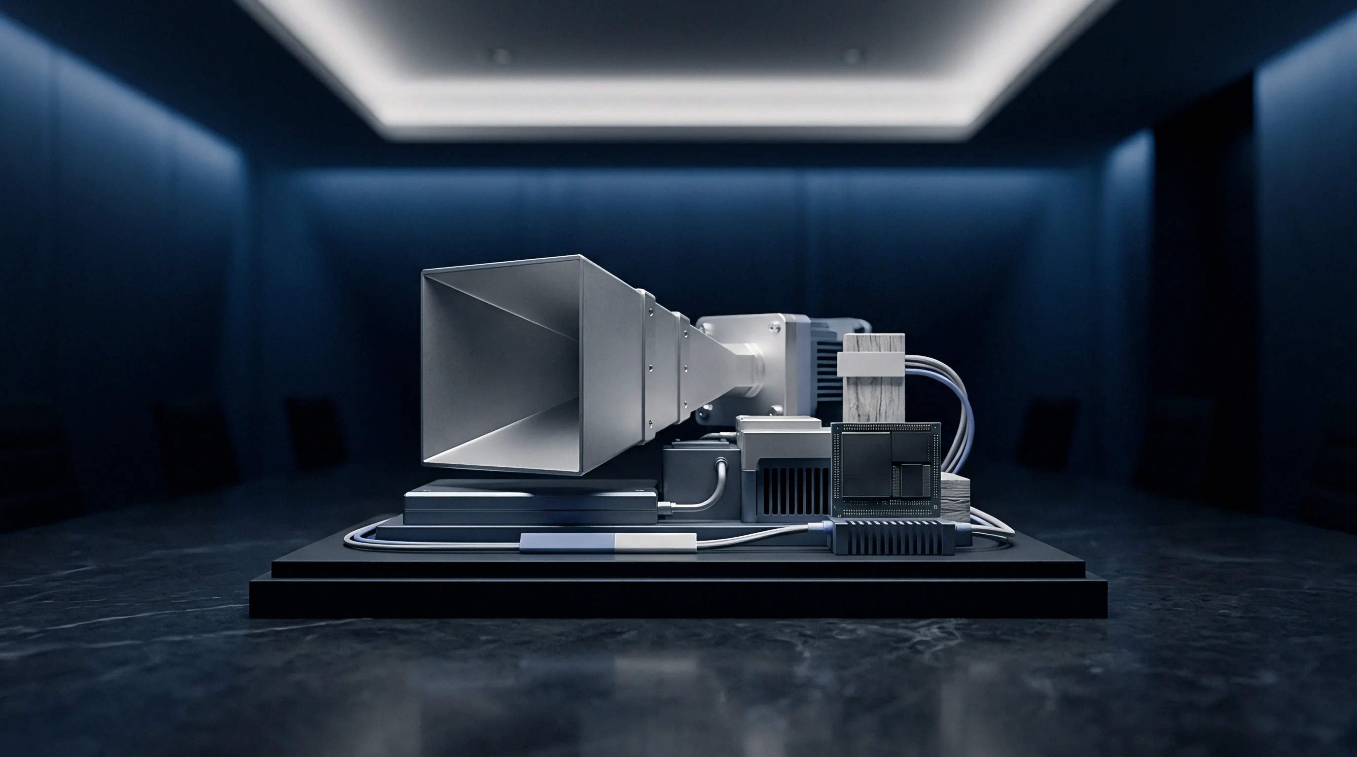
The diagram below illustrates the physical connections and instrument routing required for automated thermal timing verification.
Power profiling hardware measures current consumption synchronously with digital logic analyzer traces. By mapping current consumption spikes to micro-controller operational phases, test engineers verify whether extended receiver guard windows consume excessive battery charge under thermal stress. Automated test scripts ramp environmental chamber temperatures while logging clock phase offset relative to a rubidium-standard reference clock, generating statistical drift distributions across hundreds of consecutive sleep cycles.

Statistical Bucket Validation under Thermal Cycling
Validating sliding window alignment requires evaluating thousands of sequential sleep-wake cycles under continuous thermal stress. A single pass-fail test at room temperature provides no insight into system reliability across field operating environments. Statistical validation measures three primary metrics: mean bucket offset, phase variance, and maximum clock jitter under worst-case thermal slopes.
Test software logs the precise arrival time of every transmitted telemetry packet relative to ground-truth time managed by the test controller. The calculated phase error for each cycle populates a rolling statistical distribution. The table below illustrates typical benchmark measurement outputs collected during thermal cycling tests of crystal-less nodes versus quartz-referenced nodes.
| Evaluation Metric | Uncompensated Internal RC | Polynomial-Compensated RC | Standard 32.768 kHz Quartz |
|---|---|---|---|
| Mean Timing Offset (1 Hour Sleep) | 108.4 seconds | 2.16 seconds | 0.036 seconds |
| 3-Sigma Phase Variance (Jitter) | +/- 14.2 seconds | +/- 0.45 seconds | +/- 0.008 seconds |
| Max Observed Bucket Drift (24 Hours) | 2710 seconds | 54.2 seconds | 0.86 seconds |
| Required Guard Window Width | 120.0 seconds | 3.0 seconds | 0.05 seconds |
| Average Battery Current Impact | + 420 % baseline | + 12 % baseline | + 3 % baseline |
Analyzing empirical bench data confirms that uncompensated internal RC timing causes severe sliding window misalignment, rendering nodes incapable of maintaining sync without minute-wide guard windows. Implementing polynomial thermal compensation brings phase variance within acceptable limits for low-duty-cycle protocols, allowing guard windows to shrink down to a few seconds. The residual phase error observed under rapid thermal ramps highlights the operational limit of software-only timing approaches.
Silicon vendors often claim internal RC oscillators maintain high accuracy across operating ranges, but critical examination of their datasheet conditions reveals those figures assume constant supply voltages and zero thermal gradients.
Appraisal
Designing crystal-less wireless nodes requires balancing immediate hardware savings against long-term energy penalties and field operational risks. Eliminating an external 32.768 kHz quartz crystal, along with its associated load capacitors, cuts direct bill-of-materials cost by $0.08 to $0.16 per unit in high-volume production. In multi-million unit deployments, these component savings represent significant initial capital reductions.
Omitting the crystal eliminates assembly yield loss linked to crystal oscillator circuit layout sensitivities, such as stray PCB trace capacitance, solder flux contamination leakage, and mechanical cracking caused by physical shock or vibration.
This initial component savings must be weighed against the ongoing energy cost of wider RF receiver guard windows. Operating an active radio receiver to absorb large timing uncertainties drains energy from non-rechargeable battery cells. A node that opens its receiver 3 seconds early to catch periodic network anchor frames expends significantly more milliampere-hours over its operational lifespan than a node equipped with an accurate quartz crystal that wakes up 50 milliseconds early.
The developer either pays for the crystal up front or pays for a larger battery cell to sustain extended guard window current consumption over time.
Bill of Materials versus Battery Airtime Balance
Quantifying the financial trade-off between component costs and battery capacity requires lifetime energy accounting models. Consider a smart water meter designed for a 10-year field service lifespan powered by a primary Lithium Thionyl Chloride (LiSOCl2) AA battery cell rated at 2,400 milliampere-hours. The meter reports hourly flow totals using 15-minute sliding aggregation buckets and synchronizes its clock via daily network anchor frames.
The table below models the financial and technical trade-offs across three clocking architecture options.
| Architecture Option | Initial BOM Cost Additive | Daily Guard Window Airtime | 10-Year Energy Consumption | Required Battery Cell Size |
|---|---|---|---|---|
| Option A: Crystal-Less (Uncompensated) | $0.00 (Baseline) | 2880 seconds / day | 4800 mAh (Exceeds 1x AA) | 2x AA Cells ($2.40 extra) |
| Option B: Crystal-Less (Polynomial Compensated) | $0.02 (Cal Flash Cost) | 72 seconds / day | 2150 mAh (Fits 1x AA) | 1x AA Cell ($0.00 extra) |
| Option C: Hardware 32.768 kHz Quartz Crystal | $0.12 (Crystal + Caps) | 1.2 seconds / day | 1850 mAh (Fits 1x AA) | 1x AA Cell ($0.00 extra) |
The economic analysis demonstrates that an uncompensated crystal-less design fails to meet a 10-year operating lifespan on a single AA battery cell. The energy spent running wide receive guard windows doubles total capacity requirements, forcing the inclusion of a second battery cell that costs far more than the omitted crystal. Implementing software polynomial compensation successfully recovers battery lifespan, enabling the node to run on a single battery cell while preserving initial bill-of-materials savings.
Option B offers the lowest total landed cost, provided the deployment environment remains within the bounds of the polynomial compensation model.
Evaluating protocol options across destination geographic markets forms the final step in selecting clock architectures. European sub-GHz regulations enforce strict 1 percent hourly duty-cycle ceilings under ETSI EN 300 220 rules. A node operating without a crystal that miscalculates its local sliding window boundary risks exceeding legal duty-cycle caps, triggering regulatory non-compliance fines or network bans.
In North American markets operating under FCC Part 15 regulations, frequency-hopping spread-spectrum rules mandate precise dwell times across available channels. Misaligned clocks cause channel hopping failures, increasing packet error rates and forcing costly retransmissions.
Geographic Band Ceiling and Protocol Risk
Wireless modules entering international distribution must pass regional compliance certifications with their target clock architectures fully enabled. Testing laboratories evaluate duty-cycle compliance, spurious emissions, and channel hopping behavior under extreme temperature limits inside thermal test chambers. A crystal-less design that drifts out of compliance at minus 20 degrees Celsius fails type approvals, blocking product entry into cold-climate target regions.
To reduce risk when specifying crystal-less clock systems for international markets, engineers write strict qualification clauses into sourcing contracts:
- Thermal Drift Limits specify maximum allowable clock drift across the full operating range, such as post-compensation drift under 500 ppm from -40C to +85C.
- Guard Window Bounds set strict upper limits on active receiver guard windows during network anchor frame acquisition, preventing unexpected battery drain.
- Factory Calibration Verification mandates 100 percent factory testing and logging of thermal polynomial coefficients into non-volatile device memory.
- Regulatory Duty-Cycle Margin enforces a minimum 15 percent safety margin below regional duty-cycle limits to absorb phase errors under thermal swings.
Product teams choosing between hardware crystals and software-compensated RC oscillators must evaluate full system lifetime costs rather than focusing solely on upfront component prices. When software developers implement robust polynomial compensation, verify drift bounds across thermal chambers, and maintain adequate guard margins, crystal-less architectures achieve reliable sliding window synchronization without sacrificing battery life or market access.