Meaning
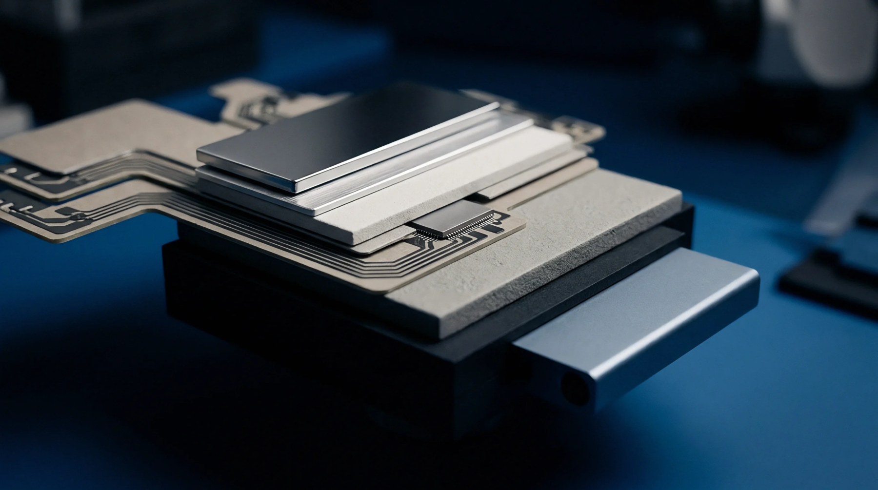
Metal redistribution layers on a silicon interposer connect high density chiplet I/O ports to a primary substrate board. 2.5d interposer routing establishes the physical paths required to break out fine pitch connections from an advanced processor or memory die to the broader grid of a printed circuit board. This architecture relies on thin film fabrication techniques to overcome the pitch mismatch between dense die pads and standard packaging interfaces.
Interconnect Topology
Designers optimize signal traces to manage electromagnetic interference and impedance control across the silicon surface. High bandwidth memory modules require precise trace spacing to prevent crosstalk while maintaining timing synchronization between multiple components. Each path across the substrate undergoes simulation to verify that signal integrity meets the required gigabit thresholds.
Thermal management dictates the maximum routing density because trace congestion limits heat dissipation from the active silicon die.
Manufacturing Constraint
Fabrication facilities employ photolithography processes analogous to semiconductor production to build the multi-layer dielectric structure. Copper pillar density limits the available routing channels, forcing a balance between chiplet size and the number of available signal paths. Precise alignment of these microscopic vias determines the final yield of the assembly process.
Small shifts during layer deposition result in short circuits that render the entire module unusable.
Validation Protocol
Engineers confirm the functionality of the routing paths through electrical testing after the assembly of the silicon interposer onto the host substrate. Automated probes verify continuity and resistance for each signal net to ensure the connection matches the design intent. A failed path at this stage typically necessitates the rejection of the entire multi-chip package.
Successful operation depends on the precision of the underlying metal patterns.