Meaning
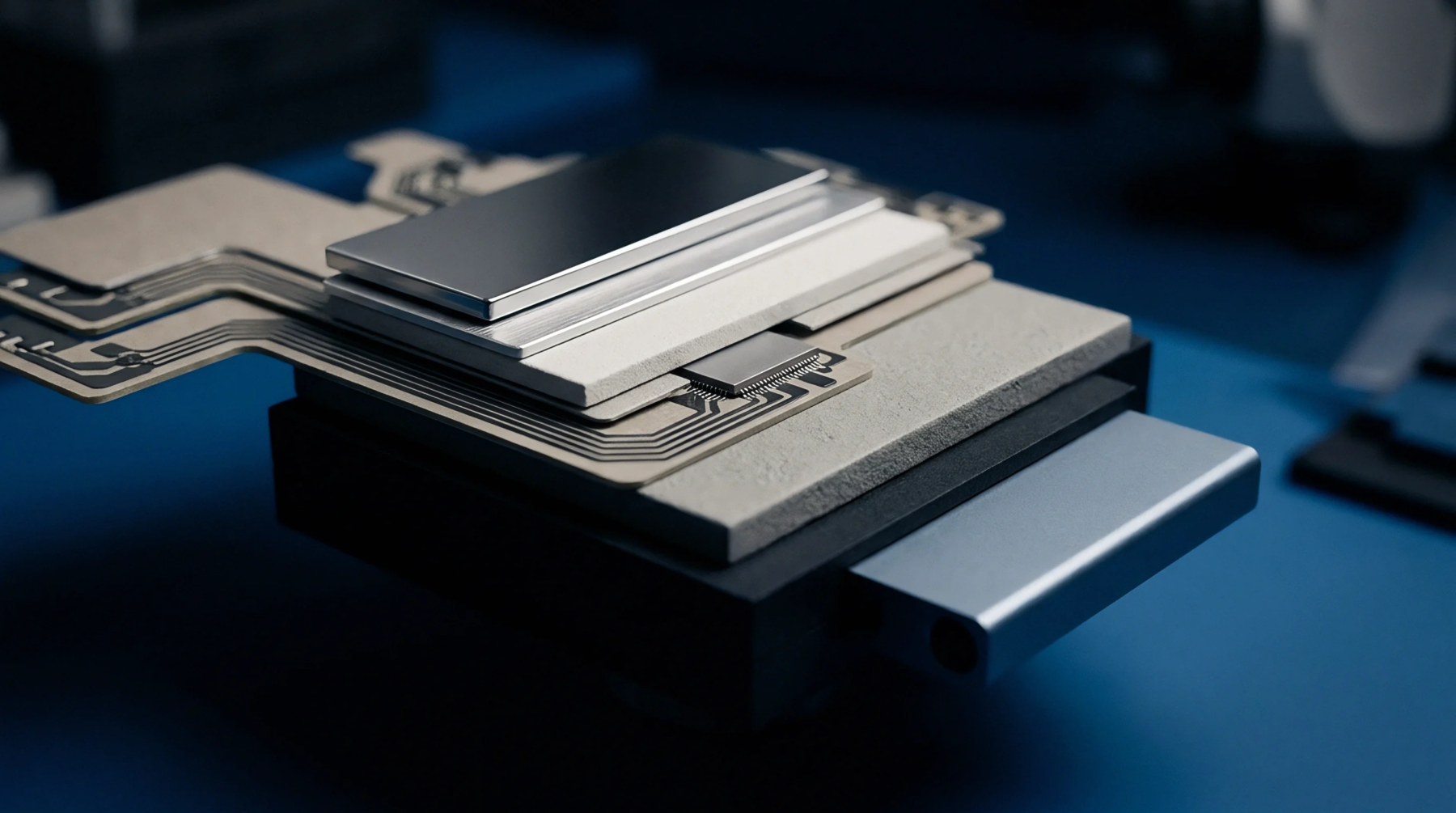
Copper redistribution layer intellectual property provides the physical routing structure that bridges sub-micron integrated circuit bond pads to coarser pitch substrate bumps within advanced packaging architectures. Manufacturing flows deposit dielectric layers and copper traces on the wafer surface to fan out input and output signals beyond the tight pitch of the silicon die. Electrical performance depends directly on the parasitic capacitance and resistance introduced by these thin film metal lines during high frequency signal propagation.
Dielectric thickness and trace spacing govern the electrical isolation between adjacent routing channels, preventing crosstalk and signal degradation across the package boundary. The redistribution layer intellectual property defines the exact photomask layout rules, design rule checks, and process integration parameters required to fabricate these high density interconnects without introducing yield-limiting defects.
Routing Density
Modern packaging demands ultrafine trace dimensions to accommodate thousands of input and output terminals on a single application processor die. Design teams license redistribution layer intellectual property to establish pitch scaling limits and metal thickness ratios that survive mechanical thermal cycling without copper delamination. High density fan-out wafer level packaging relies on these predefined routing specifications to fan out signals to a ball grid array with a pitch exceeding eight hundred micrometers.
Microvia placement rules within the intellectual property package dictate how signal traces transition between multiple metallization layers without exceeding local thermal dissipation budgets.
Thermal Stress
Mechanical reliability testing evaluates how coefficients of thermal expansion mismatch between silicon, molding compound, and organic substrates affect redistribution layer copper traces. Temperature cycling tests expose packaged assemblies to extreme thermal ranges, measuring shifts in electrical resistance that indicate micro-cracking within the fine pitch metal lines. Redistribution layer intellectual property includes material stacking guidelines and stress relief structures designed to absorb plastic deformation during operational heating cycles.
Finite element analysis models provided within the license package predict warpage and plastic strain under specific thermal loads before physical silicon touches the assembly line.
Supplier Qualification
Foundry qualification protocols verify whether a fabrication house can reproduce the specified redistribution layer intellectual property patterns within acceptable yield thresholds. Scanning electron microscopy and cross-sectioning inspect metal line sidewall profiles and dielectric planarization quality after chemical mechanical polishing steps. Buyers evaluate these physical verification reports alongside electrical parametric test results to confirm that the licensed intellectual property matches the performance of the assembled semiconductor product.
End-customer acceptance depends entirely on passing these rigorous back-end manufacturing audits without exceeding allowable trace resistance variations across the entire wafer surface.