Structuring Cross Border Foreground Patent Indemnification across Multi Tier Semiconductor Assembly Supply Chains
Structuring cross-border packaging indemnification demands uncapped IP liability carve-outs, IPC-2581 design escrow, and unbroken sub-tier flow-down covenants.


Scope
Semiconductor packaging contracts often fail to align intellectual property risks between turn-key integrators and original equipment manufacturers. When a multi-chip module combines silicon IP from three separate countries inside one multi-tier substrate, financial liability ultimately hinges on which party owns the novel assembly structures. Turn-key sourcing transfers baseline obligations to the primary vendor, but semi-custom design flows complicate matters by introducing buyer-specified redistribution routing and custom substrate interposers.
Defining the boundary between background intellectual property and foreground patent creation requires precision long before silicon ever hits the assembly line.
Background intellectual property covers pre-existing semiconductor process patents, standard packaging configurations, standard cell design libraries, and baseline substrate stack-up options held by foundries or Outsourced Semiconductor Assembly and Test entities. Foreground IP is created specifically during module design, customization, and physical assembly ~ covering non-standard redistribution layer geometries, physical chiplet placement profiles, custom solder bump arrays, thermal spreader attachment mechanisms, and specialized firmware integration code. Disputes frequently arise in cross-border procurement when an assembly partner claims background ownership over structural adaptations built specifically to meet a buyer’s engineering specs.
Ninety percent of standard packaging agreements across Taiwanese and South Korean OSAT partners silently attempt to capture custom interposer routing as foundry background IP. Buyers signing standard manufacturing terms without clear foreground patent allocations forfeit the right to patent their own structural package innovations. Worse, they leave themselves exposed to infringement suits if the vendor re-uses those exact physical structures in modules built for direct competitors.

Defining Foreground Patent Claims in Heterogeneous Assemblies
Heterogeneous packaging combines silicon dies fabricated at different technology nodes into one functional package. A multi-chip module might bring together a 4-nanometer digital application-specific integrated circuit, a 16-nanometer analog front-end, and two high-bandwidth memory stacks on a silicon interposer. Infringement claims in this space rarely target the internal transistor structures of individual dies; patent assertion entities focus on the physical interconnections, power distribution networks, and packaging features introduced during assembly.
Foreground patent creation in heterogeneous packaging generally concentrates across three physical layers:
- Interposer Metallization Geometries includes novel trace widths, spacing profiles, and differential pair routing patterns etched into the silicon or organic interposer layer to manage high-speed signaling between heterogeneous dies.
- Thermal Interface Attachments covers custom package lids, heat slug profiles, micro-channel liquid cooling passages, and specialized phase-change material applications integrated into the top packaging layer.
- Substrate Power Plane Topologies defines specialized copper pour shapes, embedded decoupling capacitor cavities, and vertical via array distributions designed to minimize voltage drop across high-current die domains.
When an engineering scope requires a custom interposer, the buyer’s internal team typically creates the initial layout topology. If the OSAT then performs physical routing enforcement and design rule checking, both parties end up contributing to the final manufacturing dossier. Unless the procurement agreement explicitly assigns all resulting foreground packaging patents to the buyer, the OSAT can file patent applications on those interposer layout rules ~ creating immediate conflict if the buyer later tries to move the package design to a second-source assembly facility in another jurisdiction.
Incorporating IPC-2581 design transfer specifications directly into the warranty schedule converts ambiguous layout representations into strict structural boundary definitions that bar extraneous infringement claims.
Multi Tier Liability Boundaries from Foundry to System Integrator
The semiconductor assembly supply chain is a multi-tier hierarchy. Raw material suppliers providing copper foils, epoxy mold compounds, and organic laminates sit at the base. Above them are pure-play silicon foundries producing processed wafers, substrate manufacturers fabricating high-density interconnect cards, and OSAT houses performing wafer sorting, dicing, die attach, wire bonding, flip-chip assembly, and final testing.
At the top, the turn-key module integrator delivers a finished, qualified module to the original equipment manufacturer.
Indemnification across this chain depends entirely on contract privity. A wafer foundry has a direct contract with the fabless chip designer, while the OSAT deals strictly with whoever places the assembly purchase order. If a patent assertion entity files suit alleging that a micro-bump alloy composition violates a regional package patent, the OEM faces immediate pressure and demands defense from the turn-key module integrator.
Yet the module integrator cannot pass that liability down to the sub-tier OSAT unless explicit flow-down provisions exist in the underlying supply contracts.
Substrate boundaries often determine ultimate liability. Turn-key integrators frequently limit their indemnification obligations to their direct physical additions, excluding third-party silicon dies and raw substrates. This leaves a major coverage gap for the buyer.
If a third-party IP core inside a custom ASIC infringes a patent, or if the substrate vendor’s via-drilling process violates a patent, the turn-key integrator disclaims responsibility. The buyer absorbs the risk of injunctions and damages despite paying full turn-key margins.
Binding suppliers through strict IPC-2581 design transfer specifications establishes clear structural boundaries in the contract, preventing layout ambiguities from escalating into external infringement claims.


Die
Silicon interconnect assemblies introduce distinct patent risks right at the physical packaging boundary. Advanced packaging has shifted much of semiconductor innovation from sub-micron transistor gate dimensions to millimeter-scale structural integration. As physical die shrinkage slows, assembly houses rely on 2.5D interposers, 3D wafer stacking, high-density redistribution layers, and fan-out wafer-level packaging to drive functional density.
These packaging methods create dense networks of cross-border foreground patents that target physical structures rather than logical circuit designs.
When reviewing substrate layer routing, ambiguity around who indemnifies redistribution layer patents comes up constantly. Redistribution layers route electrical signals from tight-pitch silicon pads to wider-pitch substrate pads via deposited copper traces and dielectric layers. OSAT houses hold extensive background patent portfolios covering their specific chemical vapor deposition steps, photoresist coating processes, and seed-layer etching routines.
However, the physical layout of those traces relative to specific component pads forms a unique geometric arrangement. Patent assertion entities target these geometric layouts, alleging infringement against the physical module layout rather than the underlying chemical process.
Custom interposers bring separate patent risks. High-density interposers use silicon, glass, or organic cores to run thousands of parallel connections between adjacent dies. The physical construction of Through-Silicon Vias, micro-bump pads, and integrated passive devices within the interposer substrate regularly touches third-party patent portfolios.
Anyone specifying a semi-custom interposer stack-up has to establish whether exposure stems from physical substrate fabrication steps or the layout pattern provided by their own physical design team.

Silicon Packaging Mechanics and Physical IP Substrates
Physical semiconductor packaging relies on structural engineering principles that assertion entities can analyze using non-destructive physical inspection. Infrared microscopy, high-resolution X-ray computed tomography, and scanning electron microscopy let competitors examine internal package geometries without destroying the device. This visibility makes packaging features accessible targets for litigation.
Unlike internal firmware algorithms or software logic, physical structures provide visual evidence of infringement as soon as a product hits the market.
Physical packaging features generating the highest density of cross-border patent disputes include:
- Micro Bump Metallurgy involves specific copper-tin-silver alloy ratios, barrier metal diffusion layers, and intermetallic compound thicknesses at the die-to-interposer interface.
- Redistribution Layer Topology covers trace cross-sectional profiles, dielectric layer thickness ratios, and via pad overlap geometries within thin-film packaging layers.
- Substrate Cavity Assemblies defines recessed pockets in multi-layer organic substrates designed to house surface-mount passive components directly beneath high-power silicon dies.
- Encapsulation Mold Stress Relief includes physical grooves, mechanical lock structures, and graded filler material distributions within epoxy mold compounds designed to mitigate coefficient of thermal expansion mismatches.
Separating structural IP from functional circuit IP is essential when drafting indemnification terms. Functional circuit IP protects logical operations executed by transistors inside the silicon die, such as a hardware cryptographic engine or bus interface decoder. Structural IP protects the physical arrangement of conductors, insulators, and mechanical supports holding those dies together.
Foundries generally supply silicon dies with baseline functional IP warranties, but OSAT houses regularly disclaim structural IP indemnification for packages built to customer specs.
Interposer Geometry and Redistribution Layer Exposure
The shift to fan-out wafer-level packaging replaces traditional fiber-reinforced organic substrates with thin-film redistribution layers applied directly to dicing-grid reconstituted wafers. This approach yields high line and space density, frequently dropping trace width and spacing below 2 micrometers. Achieving that density requires process steps that overlap heavily with patented semiconductor process flows held by major IDMs and pure-play foundries.
Subtier vendors routinely push back on unconditional flowdown clauses. An OSAT fabricating a custom fan-out redistribution layer relies on proprietary process rules governing maximum metal density, copper trace dummy fill patterns, and corner stress relief radii. If a buyer mandates a specific high-density bus layout that forces the OSAT to modify its standard dummy fill algorithm, the resulting substrate may violate a competitor’s chemical-mechanical planarization patent.
Pinpointing whether liability sits with the buyer’s bus architecture or the OSAT’s modified process routine requires thorough forensic design audits.
| Assembly Tier | Technology Node / Interface | Primary Foreground IP Risk | Typical Indemnity Scope | Carrier Allocation |
|---|---|---|---|---|
| Wafer Foundry | Sub-7nm Logic Dies | Standard cell layout, TSV via-first process patents | Limited to baseline process flow | Foundry defense default |
| IP Core Licensor | SerDes / Memory Controllers | PHY interface topology, pinout geometries | Carved out from package layout | Licensor holds IP pool |
| Substrate Supplier | Build-Up Organic Laminates | Via stack structures, copper foil micro-roughness | Disclaimed for custom stack-ups | Pass-through to OSAT |
| OSAT Assembly | 2.5D Silicon Interposer | RDL trace profiles, micro-bump alloy diffusion | Restricted to standard process rules | Split joint defense |
| Module Integrator | Turn-key Multi-Chip Module | Overall system assembly, thermal spreader topology | Full OEM hold-harmless warranty | Primary liability holder |
Structural interposer patents carry serious cross-border complications because interposers are often manufactured in one country, integrated into multi-chip packages in another, and mounted onto mainboards in a third. A patent granted in Japan covering silicon interposer decoupling structures applies to assembly in Taiwan if the Taiwanese OSAT imports Taiwanese-made interposers using Japanese IP. If the finished module is then shipped to the United States, it faces potential import blocking under International Trade Commission proceedings.
Mapping the geographic footprint of interposer IP creation is an essential part of supply chain due diligence.
Unexpected thermal stress failures in custom chiplet interposers can stem from host board bending rather than proprietary redistribution layer metallization.

Nexus
Cross-border supply chains expose semiconductor modules to multi-jurisdictional patent actions. Producing a single multi-chip module often spans four countries before final assembly. Silicon wafer fabrication might happen in Taiwan, substrate manufacturing in South Korea, final OSAT assembly and test in Malaysia, and module integration in Vietnam.
This geographic spread creates tricky questions around which legal framework governs infringement, foreground IP assignment, and indemnity enforcement.
Patent rights remain strictly national. A patent granted by the United States Patent and Trademark Office offers no direct protection in Malaysia or Vietnam. If an assertion entity holds a Malaysian patent covering a die-attach adhesive curing method, the Malaysian OSAT violates local law by running that step in Malaysia.
An OEM importing the finished module into the United States does not directly infringe the Malaysian process patent on US soil. However, the OEM can still face indirect infringement claims or import exclusion orders under administrative customs laws if the imported product was manufactured abroad using a process patented in the destination market.
Packaging patents move across borders easily. Administrative trade agencies have statutory authority to block imports of goods produced abroad using processes that violate domestic patents. In the United States, Section 337 of the Tariff Act of 1930 lets the International Trade Commission investigate unfair import practices, including patent infringement.
Unlike district court litigation, which can take years of discovery to produce damage awards, ITC investigations move fast and can issue exclusion orders directing Customs and Border Protection to block infringing modules at every port of entry.

When Packaging Technology Triggers Import Exclusion Orders?
Exclusion orders halt customs entry immediately. When an International Trade Commission exclusion order arrives at a port of entry, inspectors do not review software code or evaluate contractual liability terms. Customs officers stop incoming shipments of targeted multi-chip modules based strictly on part numbers, customs codes, and package markings.
An exclusion order hitting a key power management module can shut down an entire automotive mainboard line, causing disruption far beyond the monetary value of the patent itself.
Cross-border patent enforcement strategy requires tracking foreign legal mechanisms:
- United States ITC Section 337 Orders blocking entry of downstream products containing infringing semiconductor packaging or interposer structures regardless of assembly location.
- Unified Patent Court Injunctions in Europe granting pan-European preliminary injunctions against module importers based on validated regional packaging patents.
- Taiwanese IP and Commercial Court Actions securing rapid evidentiary preservation orders directly inside OSAT cleanrooms to seize assembly routing files and batch records.
- Chinese Specialized IP Court Rulings issuing behavior preservation injunctions that restrict domestic packaging houses from exporting disputed module assemblies to overseas integrators.
Moving assembly operations to lower-cost regions alters patent risk overnight. When a primary contractor moves OSAT operations from Taiwan to Malaysia or Vietnam to dodge trade tariffs, physical assembly shifts into distinct legal jurisdictions with different patent landscapes. Malaysia and Vietnam maintain separate patent registers, court systems, and treaty obligations.
A packaging method unencumbered by patents in Taiwan might infringe active patents held by regional competitors in Southeast Asia. Contracts must be re-evaluated whenever assembly locations change within the supply network.
Achieving complete indemnity recovery across Asian OSAT nodes requires registering English-language arbitration covenants in regional legal centers with reciprocal treaty enforcement mechanisms.

Territorial Coverage Gaps in Multi Country Assembly Chains
Enforcing indemnification agreements against overseas packaging vendors often involves significant legal friction. A Western OEM might hold a solid contract with clear hold-harmless terms signed by a Taiwanese module integrator. But if a patent assertion entity sues the OEM in a German court over a European package patent, forcing that defense back onto the Taiwanese integrator requires navigating international procedures under the Hague Convention.
Audits of Asian OSAT agreements show that under fifteen percent contain explicit submission clauses to European or North American courts. When an OEM tries to join a foreign assembly house to a domestic patent suit, foreign courts often reject jurisdiction unless local-law-compliant jurisdiction covenants were executed during contract formation.
Contractual indemnification language must bridge geographic enforcement gaps using dedicated international arbitration clauses. Standard domestic courts operate inefficiently across borders. Establishing International Chamber of Commerce or Singapore International Arbitration Centre arbitration seats within the master agreement ensures disputes are handled under neutral, enforceable frameworks like the New York Convention on the Recognition and Enforcement of Foreign Arbitral Awards.
This allows an OEM to turn an indemnification award against a foreign OSAT into enforceable asset attachments wherever that OSAT holds manufacturing assets or bank accounts.
Failing to align assembly country designations with regional patent portfolios causes immediate customs detentions that freeze entire retail product distribution channels without contractual defense recourse.


Cap
Liability terms in semiconductor manufacturing contracts govern how financial damages flow between assembly tiers. Under standard commercial terms, component vendors usually try to limit aggregate liability to the net amount paid by the buyer for units delivered over the preceding twelve-month period. For low-cost commodity parts, that fee-based cap offers reasonable risk boundaries for the supplier.
In custom multi-chip packaging, however, applying a standard fee-based cap leaves the buyer heavily exposed to major litigation costs.
Uncapped defense liabilities erode module margins quickly. A custom high-density module priced at forty dollars might bring in two million dollars in annual billings for the OSAT. If an assertion entity sues the OEM over that module, legal defense fees alone regularly cross three million dollars before trial, while damages tied to finished-product margins can reach tens of millions.
If the OSAT’s indemnity obligation is capped at its two-million-dollar trailing revenue, the OEM absorbs the remaining deficit despite having paid a turn-key premium for complete module delivery.
Carving out patent indemnification from standard liability caps is mandatory in high-reliability semiconductor procurement. Standard commercial caps fit operational defect claims, late delivery penalties, and quality failures. Patent claims, by contrast, are external third-party actions that scale with finished-product retail prices rather than component costs.
Custom semiconductor contracts must therefore set separate, expanded liability limits ~ or uncapped obligations ~ specifically for intellectual property indemnification.

Structuring Pass through Indemnity Covenants across Subtiers
Pass-through indemnity structures attempt to place contractual liability directly on the tier that introduced the patent risk. A turn-key module integrator sourcing silicon dies from a foundry, substrates from a laminate supplier, and assembly from an OSAT acts as a system consolidator. If an infringement claim targets an internal substrate via structure, the module integrator tries to pass that liability down to the substrate supplier who engineered the laminate layer.
Effective pass-through indemnity architectures rely on specific structural mechanics:
- Unbroken Privity Clauses requiring every sub-tier supplier contract to mirror the master IP indemnity language and defense performance standards established between the OEM and primary integrator.
- Super Cap Allocations establishing explicit liability limits for patent claims set at five to ten times annual contract value rather than trailing twelve-month revenues.
- Immediate Defense Substitution permitting the OEM or primary integrator to step in and assume direct legal control of patent defense litigation if a sub-tier supplier delays legal appearance.
- Indemnification Escrow Holdbacks retaining three to five percent of non-recurring engineering milestones until sub-tier IP ownership audits and patent clearance dossiers pass verification.
Sub-tier suppliers frequently resist unlimited pass-through indemnification clauses. A small, specialized substrate house providing novel high-density organic interposers lacks the balance sheet capacity to absorb uncapped patent liabilities generated by global smartphone distribution chains. When negotiating multi-tier assembly agreements, procurement strategists must balance strict flow-down requirements against the financial reality of sub-tier vendors.
Forcing an uncapitalized vendor to sign an uncapped liability covenant yields false security; if a major infringement action lands, the sub-tier vendor simply files for corporate reorganization, leaving the primary buyer holding the entire financial loss.

Carve Outs Defense Control and Aggregate Liability Limits
Managing patent defense requires explicit rules covering who selects legal counsel, who directs litigation strategy, and who approves settlement terms. Standard supplier indemnity clauses usually state that the supplier retains sole control over defense. While that protects the supplier from inflated legal fees from high-cost law firms chosen by the buyer, it creates major conflicts of interest during active litigation.
| Tier Level | Contractual Party | Cap Structure | Defense Obligation | Carve-Out Exceptions |
|---|---|---|---|---|
| Tier 1 | Turn-key Module Integrator | Uncapped or 5x Contract Value | Primary duty to defend and indemnify | Customer-mandated custom routing |
| Tier 2 | OSAT Assembly House | 2x Annual Assembly Billings | Pass-through packaging defense | Standard background process rules |
| Tier 2 | Foundry / Die Supplier | 1x Trailing 12-Month Billings | Limited silicon process defense | Third-party IP core integration |
| Tier 3 | Substrate Manufacturer | Fixed Dollar Cap ($1M – $5M) | Substrate via layout defense | Buyer-specified material layers |
| Tier 3 | IP Core Licensor | 1x Lifetime License Fees | Logic block defense only | Modification by fabless designer |
When dual-sourcing splits foreground patent ownership and a supplier controls defense counsel, counsel’s primary duty runs to the supplier, not the buyer. A supplier facing a patent assertion entity might settle by agreeing to pay a running royalty on future component shipments in exchange for a release of past damages. That structure harms the buyer directly if the component royalty raises unit procurement costs, making the downstream product uncompetitive.
Agreements should explicitly bar suppliers from settling on terms that admit buyer liability, force unit price increases, or impose injunctions on downstream buyer distribution without express written consent.
Always match the indemnity liability limit to the maximum landed replacement value of the highest-risk single custom component rather than the annual contract volume.

Receipt
Financial mechanics in semiconductor integration contracts turn abstract patent risks into line items on an invoice. Non-recurring engineering charges, tooling fees, mask set amortizations, and yield adjustments represent the primary monetary transfers in custom assembly projects. Structured properly, these invoice mechanics work as enforcement tools for cross-border foreground IP indemnification.
Linking disbursements to patent clearance milestones prevents vendors from collecting engineering fees while handing unvetted patent exposure to the host system builder.
Structuring cross-border indemnification covenants requires binding sub-tier suppliers through flow-down agreements. Non-recurring engineering payments should never be paid out entirely upfront. Custom packaging development moves through distinct engineering phases: thermal simulation, physical interposer layout, multi-project wafer shuttle runs, substrate tooling fabrication, prototype assembly, and final qualification.
Tying NRE milestone payments to explicit patent clearance deliverables ensures the vendor produces verifiable IP documentation before receiving capital funds.
Royalty offsets help balance non-recurring engineering costs. If a third-party patent dispute forces a buyer to take a license to maintain supply, contractual royalty offset clauses let the buyer deduct those licensing fees directly from ongoing component invoices. If an OSAT’s redistribution layer infringes a patent, requiring a two-dollar royalty per module to resolve, the buyer automatically deducts two dollars from the landed unit price of every subsequent module invoice until the economic impact of that third-party license is recovered.
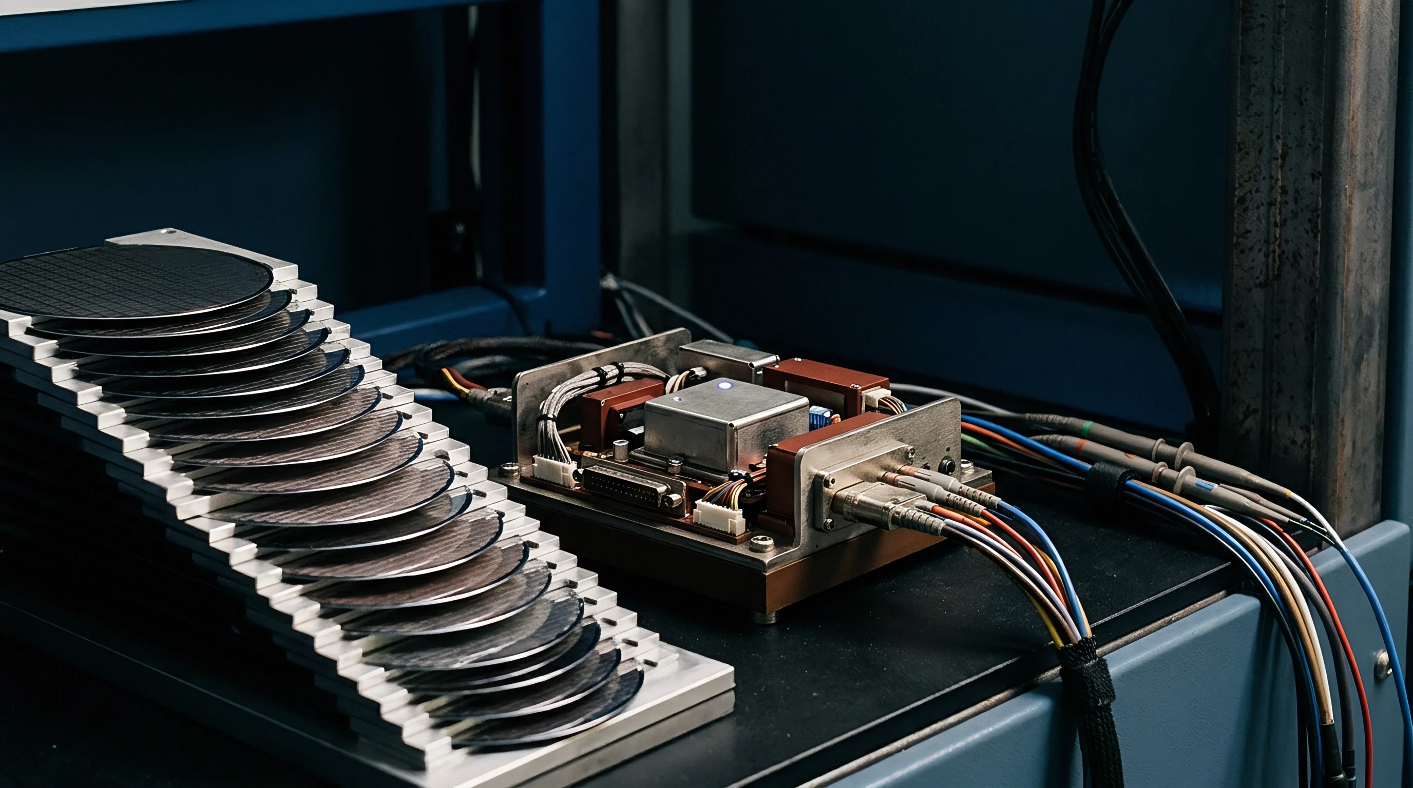
Non Recurring Engineering Amortization and Royalty Offsets
Unbundling NRE charges shows how vendors quietly shift development costs and patent indemnification risks back onto buyers. Turn-key quotes often bundle custom interposer design, mask set creation, substrate tooling, and initial bring-up into a single line item called NRE Fee. That lump sum hides whether the vendor is developing clean, proprietary foreground IP or adapting existing, encumbered background IP.
A rigorous financial breakdown of custom semiconductor NRE requires separate line items:
- Substrate Photolithography Mask Charges covering the physical photomask sets required for custom high-density redistribution layer etching and micro-bump placement.
- Forensic Patent Clearance Dossier Delivery funding formal third-party legal freedom-to-operate searches and non-infringement opinion letters covering custom packaging geometries.
- Design Rule Modification Engineering Hours paying for explicit adjustments made to standard OSAT assembly rules to accommodate unique buyer packaging requirements.
- Prototype Failure Analysis and Modification Escrow holding reserve capital to execute physical design-arounds if initial prototype units trigger third-party IP infringement assertions.
Amortizing NRE into unit pricing adds further indemnification complexity. If an OEM agrees to pay off a two-million-dollar NRE fee by adding five dollars to the price of the first 400,000 production units, the vendor carries financial risk during the early ramp. If a patent injunction stops production at 100,000 units, the vendor loses the remaining 1.5 million dollars in unamortized NRE.
Vendors frequently insert acceleration clauses mandating that all unamortized NRE becomes immediately due if production stops for any reason ~ including patent litigation. Contracts must explicitly exempt patent-injunction halts from NRE acceleration clauses.

Quantifying Multi Tier Indemnity Recovery Models
Evaluating the financial impact of a cross-border patent dispute requires walking through an active multi-tier recovery scenario. Consider a high-density graphics module integrated into an industrial computing platform. The host platform sells for 2,500 dollars, utilizing a turn-key module purchased from a primary integrator for 350 dollars.
The module contains a custom interposer fabricated by a Tier-3 substrate vendor, assembled by a Tier-2 OSAT, using silicon dies from a Tier-2 foundry.
A patent assertion entity sues the OEM, alleging that the module’s interposer via structure infringes a regional patent, demanding a 3 percent running royalty on the 2,500-dollar host platform ~ equal to 75 dollars per unit. The OEM incurs 1.2 million dollars in legal defense fees while fighting the assertion over a 100,000-unit production run.
| Dispute Trigger | Tier-1 Base Cost | Sub-Tier Recovery Ratio | OEM Net Liability | Amortization Impact |
|---|---|---|---|---|
| Uncapped Flow-Down Indemnity | $350 / unit | 100% of Legal + Royalty | $0 Direct Loss | Full NRE offset achieved |
| Fee-Capped Indemnity (12-Mo Billings) | $350 / unit | 35% Recovery ($3.5M Cap) | $5.2M Uncovered Deficit | Unamortized NRE forfeited |
| Sub-Tier Insolvency / Bankruptcy | $350 / unit | 0% Sub-tier Recovery | $8.7M Total Loss | Immediate NRE write-off |
| Negotiated Royalty Offset Clause | $275 / unit ($75 Offset) | Direct Invoice Deduction | $1.2M Defense Fee Gap | Production volume maintained |
The math shows why fee-capped indemnity models collapse under litigation stress. Under a standard fee-capped agreement, the Tier-1 integrator limits aggregate liability to trailing twelve-month revenues. If annual contract volume was 10,000 units ($3.5M revenue), the maximum indemnity payout is 3.5 million dollars.
Yet total damages across the 100,000-unit run reach 7.5 million dollars in royalties plus 1.2 million dollars in legal fees, creating an 8.7-million-dollar total claim. That 3.5-million-dollar cap leaves the OEM with a 5.2-million-dollar uncovered deficit. Without explicit pass-through covenants and uncapped IP provisions, component-level cost savings disappear quickly in litigation.
It remains uncertain whether international arbitration panels will accept indirect assembly cost allocations as recoverable damages when sub-tier packaging houses fail to disclose known third-party interposer patents.


Recourse
Resolving disputes across international boundaries requires practical tools beyond conventional court proceedings. When an assertion entity secures an injunction or files an infringement claim against a custom semiconductor package, money alone will not keep operations running. The primary goal of an operational recourse clause is protecting physical supply continuity.
Contracts should compel suppliers to execute immediate technical remedies that bypass the dispute while legal teams work through liability.
Operational remedies fall into three distinct contractual performance tiers:
- Licensing Procurement requiring the supplier to immediately acquire, at its sole expense, a fully paid-up, non-exclusive license from the patent holder enabling uninterrupted manufacturing and sales.
- Non-Infringing Redesign Performance mandating that the supplier execute an immediate design-around of the infringing packaging feature within a strictly defined, short calendar window.
- Drop-In Replacement Delivery obligating the supplier to supply fully qualified, pin-compatible alternative modules sourced from non-infringing third-party assembly streams at no additional cost to the buyer.
Design-around provisions need firm schedule triggers and performance guarantees. If a patent claim targets the routing layout of a custom interposer layer, executing a design-around means re-routing traces, creating new lithography masks, running prototype wafer batches through an OSAT, and completing full environmental stress re-qualification under JEDEC standards. That process routinely takes six to nine months.
If the contract omits strict completion timelines and financial default penalties, the supplier can drag out engineering work while downstream product shipments remain held at customs ports.

Design around Protocols and Escrow Release Triggers
Escrowed source files make second-sourcing feasible. A major risk in turn-key semiconductor procurement is vendor lock-in on manufacturing source files. When an assembly house faces an injunction or stalls on a required design-around, the buyer cannot resume production without complete technical documentation required to build the module at an alternative OSAT.
Securing effective design escrow requires placing a full design transfer package with a neutral third-party escrow agent upon final qualification milestone sign-off. The escrow agreement must include automatic release triggers tied directly to IP litigation events, vendor insolvency, or vendor failure to execute mandated design-arounds within ninety days of an infringement notice.
A forensic design escrow package for custom multi-chip modules includes:
- GDSII or IPC-2581 physical layout files defining all interposer layer geometries, via locations, and pad coordinates.
- Complete Gerber fabrication data sets, drill files, and substrate layer stack-up specifications detailing dielectric constants and copper foil thicknesses.
- Subtier bill-of-materials listings detailing exact chemical compositions of epoxy mold compounds, die-attach adhesives, and thermal interface materials.
- Test jigs, automated test equipment vector files, wafer probe maps, and final test calibration specifications required to validate replacement module production.
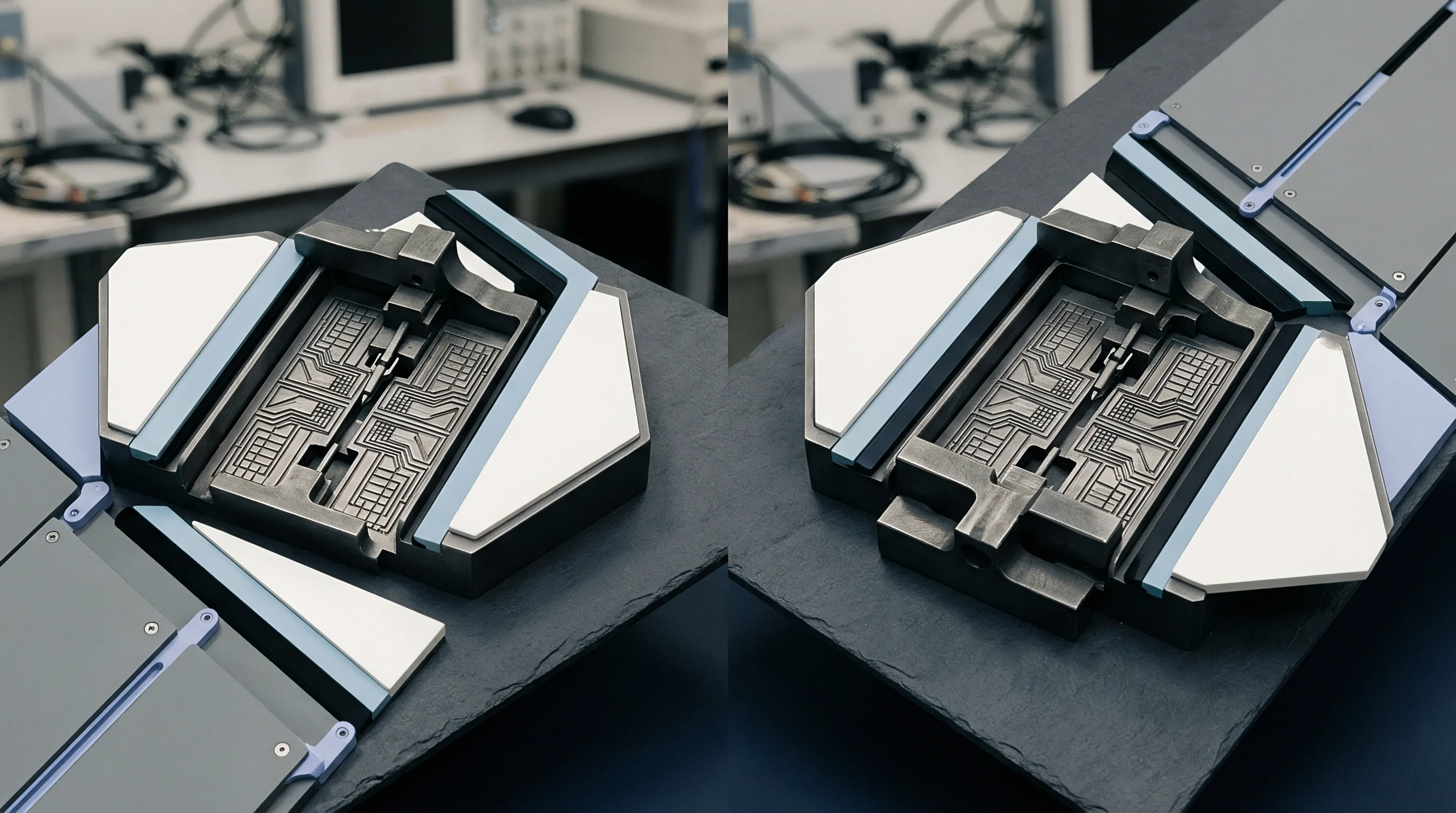
Second Source Qualification and Transfer Package Integrity
Clean design transfer packages prevent joint IP infringement when shifting production across foreign OSAT facilities. When an escrow release triggers, allowing a buyer to take interposer layout files to a second-source OSAT in a new jurisdiction, that second facility must bring up production without infringing the original OSAT’s background process patents. If the original OSAT relied on a patented seed-layer deposition technique to form micro-vias, copying the physical layout directly into a new factory might breach the original OSAT’s process rights.
Dual sourcing splits foreground patent ownership unless design transfer packages enforce absolute boundary isolation. The buyer’s engineering team must maintain strict separation between package layout specifications and factory-specific process assembly specifications. Layout specifications belong exclusively to the buyer as foreground IP, while process specifications remain vendor background IP.
By enforcing clean IPC-2581 design transfer standards, the buyer guarantees that the second-source facility receives pure geometric layout data stripped of any vendor-proprietary chemical or process steps. This boundary isolation protects the buyer from trade secret misappropriation claims while ensuring rapid, legal bring-up at alternative cross-border packaging nodes.
Foreign judgments require local court enforcement through international arbitration enforcement channels. Executing effective cross-border recourse depends on maintaining pre-qualified second-source packaging options across separate legal jurisdictions, ensuring that no single patent assertion action or regional customs blockage can freeze global supply chains.