Meaning
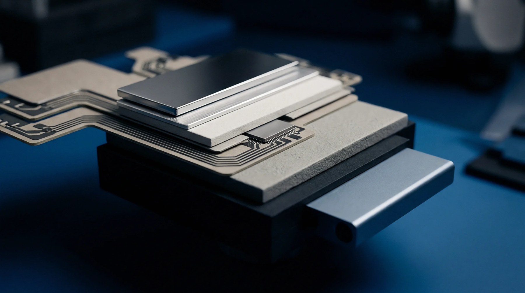
Integrated circuit assembly techniques combine multiple semiconductor dies into a single high-density enclosure to improve performance and reduce footprint. Using multi chip module packaging allows for the integration of different technologies, such as digital logic and radio frequency amplifiers, on a single substrate. This approach reduces the distance that signals must travel between components.
Interconnect Density
Placing dies closer together allows for a higher number of connections than would be possible with separate packages on a standard circuit board. In multi chip module packaging, fine-pitch wire bonds or flip-chip bumps provide the electrical path between the silicon and the carrier. This density supports faster data rates and reduces the parasitic inductance of the system.
Heat Dissipation
Concentrating multiple heat-generating components in a small area requires an efficient thermal path to the outside world. Multi chip module packaging designs often use high-conductivity ceramics or integrated heat spreaders to manage the temperature of the internal dies. Selecting the right materials for the package base is required to prevent thermal throttling of the electronics.
Assembly Yield
Testing every individual die before it is placed into the enclosure is required to maintain a high final success rate. Because multi chip module packaging involves several complex parts, the failure of a single component can result in the loss of the entire module. Advanced inspection techniques like acoustic microscopy verify the integrity of the internal bonds without damaging the assembly.