Component Substitution Notices Arriving after the Production Run
Post-production component change notices require immediate lot quarantine, parametric bench verification, and commercial debit memos under JESD46D covenants.
Physical inspection techniques involve the removal of protective packaging from an integrated circuit to expose the internal die and wire bonds for direct examination under high magnification. This decapsulation testing identifies internal defects, verifies the authenticity of a component, and helps engineers understand why a specific part failed in the field. It defines the point where a non-destructive test ends and a destructive analysis begins because the original housing of the part is permanently destroyed.
The process measures the physical integrity of the silicon and the quality of the internal connections against the original manufacturer’s design specifications. Quality labs use this method to detect counterfeit parts that may have been relabeled to appear as more expensive or higher grade components.
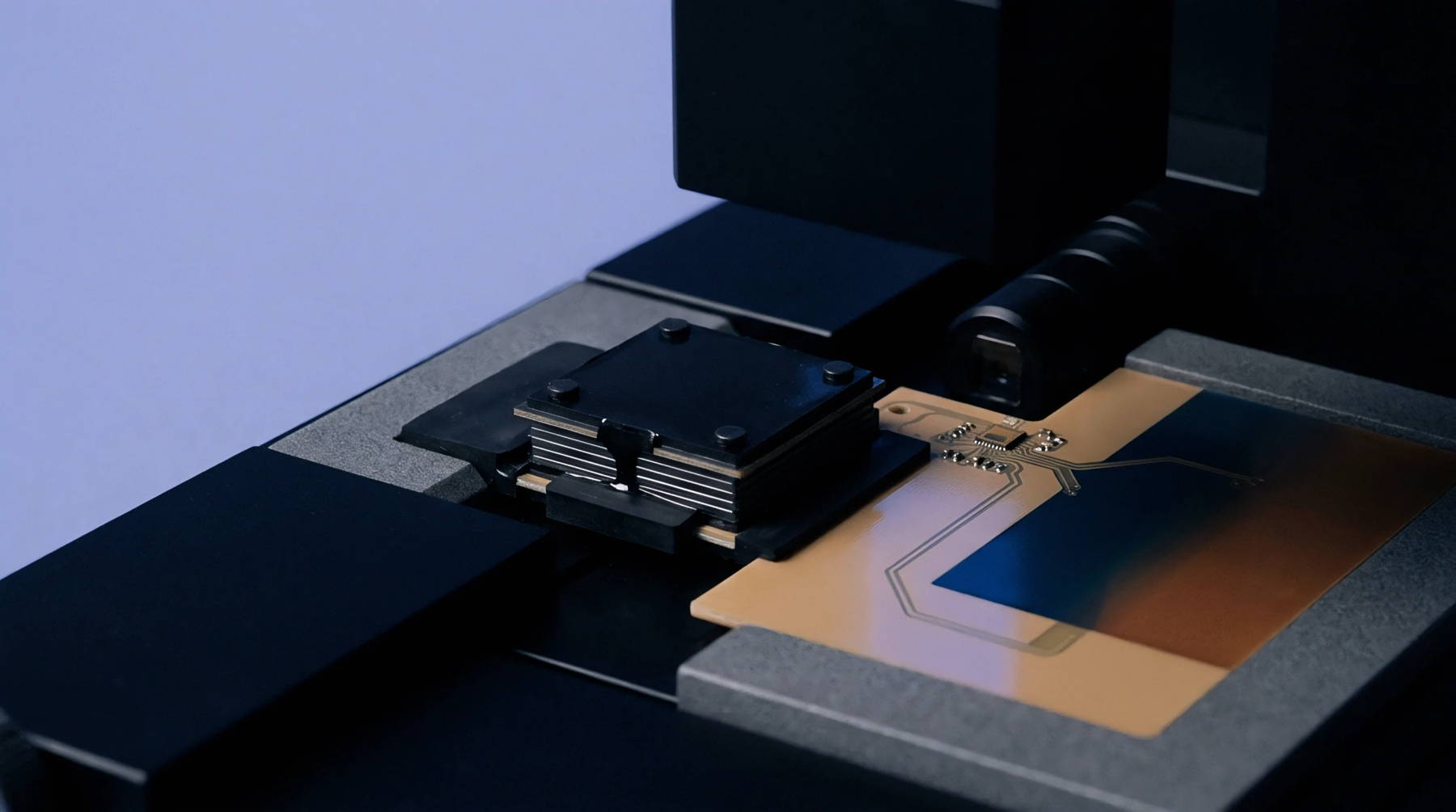
Accessing the internal structure of a semiconductor requires a controlled application of chemicals or mechanical forces to strip away the epoxy resin. During decapsulation testing, a technician usually uses fuming nitric or sulfuric acid to dissolve the plastic mold compound without damaging the silicon die or the gold bond wires. This procedure is performed in a specialized machine that regulates the temperature and the flow of the acid to ensure a clean exposure.
If the temperature is too high, the acid might etch the silicon itself and destroy the evidence of a failure. Newer methods use laser ablation to remove the bulk of the material followed by a final chemical clean to reach the delicate die surface. The goal is to create a window into the component while leaving the internal circuitry perfectly intact for the subsequent visual inspection.
Examining the exposed die allows engineers to search for physical signs of electrical overstress or manufacturing flaws. Decapsulation testing is often the only way to see a tiny burn mark or a cracked metal trace that caused a system to stop working. High power microscopes and scanning electron tools are used to look for anomalies like dendrite growth or voids in the solder balls.
If a part was damaged by a static discharge, the point of entry is often visible as a small crater on the surface of the die. These findings are documented in a formal report that includes photographs of the damage and a technical explanation of the root cause. This information is vital for the design team as they work to improve the electrical protection of the next version of the product.
Sophisticated criminals often take low cost chips and sand off the original markings to print the logos of more expensive parts. Using decapsulation testing reveals the true identity of a component by allowing the inspector to see the manufacturer’s logo and part number etched directly into the silicon. If the markings on the die do not match the markings on the external package, the part is confirmed as a counterfeit.
The test also reveals if a die has been harvested from a used circuit board and repackaged as new. This verification step is a requirement for companies building hardware for critical infrastructure or medical applications where a single fake part could lead to a catastrophic failure.
Post-production component change notices require immediate lot quarantine, parametric bench verification, and commercial debit memos under JESD46D covenants.
Expertise is a utility, not a secret. sentiention™ publishes its working knowledge as open reference: intelligence layer covering the materials it sources, the markets it enters, and the reference that serves both.