Meaning
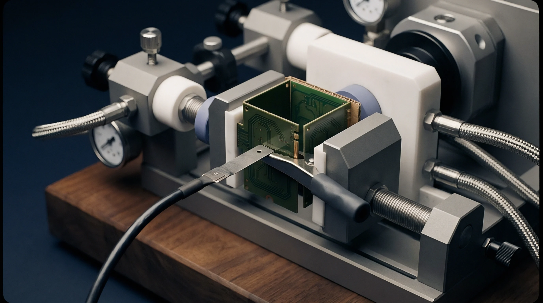
Structural arrangements of conductive copper and insulating substrate layers in a printed circuit board determine the impedance and signal integrity of high-frequency wireless designs. The dielectric stackup specifies the thickness and material properties of each insulating layer to control electromagnetic coupling between adjacent traces. This configuration forms the foundation for routing microstrip and stripline transmission lines.
Impedance Control
Maintaining a consistent trace impedance is necessary to prevent signal reflections and loss in the RF front-end circuitry. During the board design process, the dielectric stackup is calculated using the relative permittivity and thickness of the selected substrate material. If the board fabricator uses a material with a different dielectric constant, the trace widths must be adjusted to keep the impedance at the nominal fifty ohms.
This verification is completed during the design rules check before committing to volume production.
Thermal Dissipation
Heat generated by power amplifiers and microcontrollers must be efficiently transferred away from the components to the outer layers and the metal enclosure. The dielectric stackup affects this heat transfer because typical substrate materials have low thermal conductivity. Adding thermal vias that pass through the stackup layers to the ground plane helps distribute the heat and prevents localized hot spots.
This thermal management is critical to maintain the reliability of the integrated system.
Mechanical Stability
Asymmetric layer arrangements can cause the board to warp during the reflow soldering process. A balanced stackup prevents this warping and ensures a flat surface for automated component placement.