Meaning
Time-varying electric flux density passing through dielectric media generates an effective current density defined by the time derivative of the electric displacement field. This displacement current completes circuit continuity across non-conductive gaps, dielectric substrates, and free space without direct movement of physical charge carriers. The mechanism governs capacitive coupling across radio frequency board stacks and underpins electromagnetic wave launch from conductor surfaces into propagating radiation fields.
Field Conversion
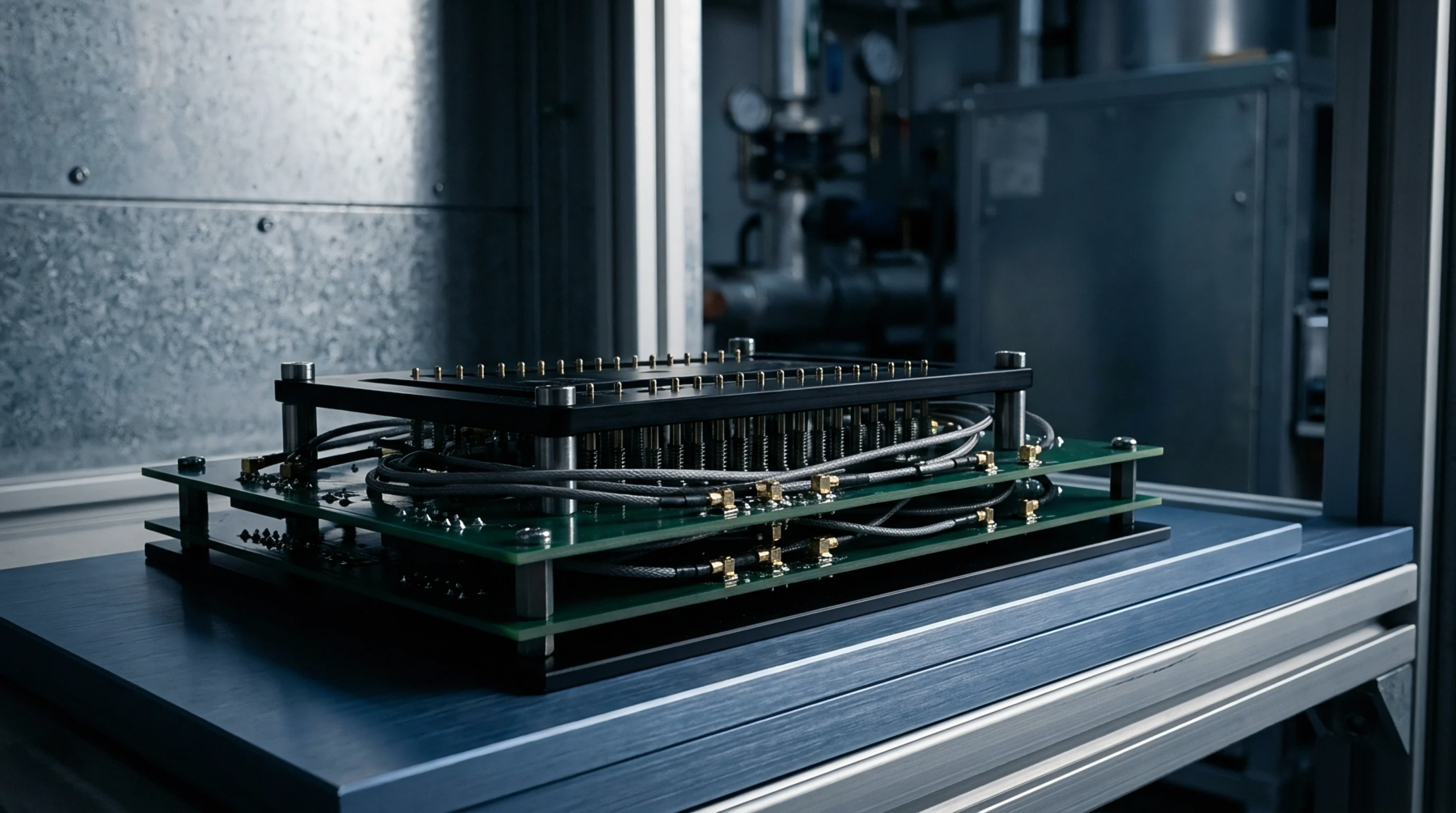
Dielectric layers separating ground planes from top-layer microstrip traces support intense time-harmonic electric fields that generate displacement current flows. These virtual currents create curling magnetic fields identical to those produced by physical conduction currents, sustaining transverse electromagnetic wave propagation along circuit board waveguides. High substrate permittivity increases total displacement density for a given electric field gradient, compressing effective operational wavelengths across printed traces.
Energy containment within controlled dielectric zones reduces unwanted stray field fringing into adjacent high-speed data circuits.
Board Coupling
Parasitic capacitance between component metallization and underlying chassis grounds allows displacement currents to bypass intended galvanic isolation barriers. Fast-switching power regulators and digital processor clock tracks launch high-frequency displacement current pulses straight through multi-layer board dielectrics into ground planes. This capacitive inject mechanism induces common-mode noise across radio frequency receiver inputs, creating in-band receiver desensitization.
Strategic via fences and localized dielectric keep-outs minimize stray displacement cross-talk between dirty digital domains and clean antenna feed structures.
Verification Protocol
High-frequency electromagnetic simulation tools compute the spatial distribution of this field quantity to identify localized capacitance hotspots prior to tape-out. Verification occurs through electromagnetic interference scanning across unshielded board prototypes during active transmit operations. Near-field magnetic sniffers detect closed-loop paths formed by displacement currents bridging trace discontinuities or PCB layer transitions.
Design sign-off requires bounding parasitic capacitive cross-talk within defined decibel margins on final hardware compliance reports.